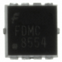
FDMC8554 Fairchild Semiconductor, FDMC8554 Datasheet - Page 2

FDMC8554
Manufacturer Part Number
FDMC8554
Description
MOSFET N-CH 20V 16.5A POWER33
Manufacturer
Fairchild Semiconductor
Series
PowerTrench®r
Datasheet
1.FDMC8554.pdf
(7 pages)
Specifications of FDMC8554
Fet Type
MOSFET N-Channel, Metal Oxide
Fet Feature
Logic Level Gate
Rds On (max) @ Id, Vgs
5 mOhm @ 16.5A, 10V
Drain To Source Voltage (vdss)
20V
Current - Continuous Drain (id) @ 25° C
16.5A
Vgs(th) (max) @ Id
3V @ 250µA
Gate Charge (qg) @ Vgs
62nC @ 10V
Input Capacitance (ciss) @ Vds
3380pF @ 10V
Power - Max
2W
Mounting Type
Surface Mount
Package / Case
8-MLP, Power33
Configuration
Single Quad Drain Triple Source
Transistor Polarity
N-Channel
Resistance Drain-source Rds (on)
0.005 Ohm @ 10 V
Forward Transconductance Gfs (max / Min)
62 S
Drain-source Breakdown Voltage
20 V
Gate-source Breakdown Voltage
+/- 20 V
Continuous Drain Current
16.5 A
Power Dissipation
2000 mW
Maximum Operating Temperature
+ 150 C
Mounting Style
SMD/SMT
Minimum Operating Temperature
- 55 C
Lead Free Status / RoHS Status
Lead free / RoHS Compliant
Other names
FDMC8554TR
Available stocks
Company
Part Number
Manufacturer
Quantity
Price
Company:
Part Number:
FDMC8554
Manufacturer:
FAIRCHILD
Quantity:
15 000
Part Number:
FDMC8554
Manufacturer:
FAIRCHILD/ON
Quantity:
20 000
FDMC8554 Rev.C
Notes:
1: R
2: Pulse Test: Pulse Width < 300µs, Duty cycle < 2.0%.
Electrical Characteristics
Off Characteristics
On Characteristics
Dynamic Characteristics
Switching Characteristics
Drain-Source Diode Characteristics
BV
∆BV
I
I
V
r
g
C
C
C
R
t
t
t
t
Q
Q
Q
Q
V
t
Q
∆V
DSS
GSS
d(on)
r
d(off)
f
rr
DS(on)
FS
GS(th)
SD
iss
oss
rss
g
∆T
∆T
g(TOT)
g(TOT)
gs
gd
rr
the user's board design.
Symbol
θJA
DSS
GS(th)
DSS
J
J
is determined with the device mounted on a 1in
Drain to Source Breakdown Voltage
Breakdown Voltage Temperature
Coefficient
Zero Gate Voltage Drain Current
Gate to Source Leakage Current
Gate to Source Threshold Voltage
Gate to Source Threshold Voltage
Temperature Coefficient
Drain to Source On Resistance
Forward Transconductance
Input Capacitance
Output Capacitance
Reverse Transfer Capacitance
Gate Resistance
Turn-On Delay Time
Rise Time
Turn-Off Delay Time
Fall Time
Total Gate Charge at 10V
Total Gate Charge at 4.5V
Gate to Source Gate Charge
Gate to Drain “Miller” Charge
Source to Drain Diode Forward Voltage
Reverse Recovery Time
Reverse Recovery Charge
Parameter
a. 60°C/W when mounted on
a 1 in
T
2
pad 2 oz copper pad on a 1.5 x 1.5 in. board of FR-4 material. R
J
2
pad of 2 oz copper
= 25°C unless otherwise noted
V
V
V
V
f = 1MHz
f = 1MHz
V
I
V
V
V
V
V
I
I
I
V
V
V
D
F
D
D
DD
GS
DD
GS
GS
GS
GS
DS
DS
GS
DS
GS
GS
= 16.5A, di/dt = 100A/µs
= 250µA, referenced to 25°C
= 250µA, V
= 250µA, referenced to 25°C
= 10V, V
= 10V, I
= 10V, R
= 10V, I
= 10V, I
= 5V, I
= 0V, I
= 16V,
= 0V
= V
= 10V, I
= 4.5V, I
= ±20V, V
2
DS
Test Conditions
, I
S
D
D
D
D
D
= 16.5A
D
GS
GEN
= 16.5A
GS
= 16.5A
= 16.5A
D
= 16.5A, T
DS
= 16.5A
= 250µA
= 14A
= 0V,
= 0V
= 0V
= 6Ω
T
J
= 125°C
(Note 2)
J
= 125°C
θJC
b. 135°C/W when mounted on a
minimum pad of 2 oz copper
is guaranteed by design while R
Min
1.0
20
2540
795
510
0.8
15.7
1.2
8.5
Typ
31
22
13
10
32
44
24
10
-6.1
1.8
3.6
4.6
5.4
7
62
3380
1060
±100
Max
765
1.3
100
24
20
51
14
62
34
47
33
θCA
3.0
5.0
6.4
7.1
www.fairchildsemi.com
1
is determined by
mV/°C
mV/°C
Units
mΩ
nC
pF
pF
pF
nC
nC
nC
nC
µA
nA
ns
ns
ns
ns
ns
Ω
V
V
V
S


