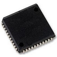
SC16C2550BIA44 NXP Semiconductors, SC16C2550BIA44 Datasheet - Page 10

SC16C2550BIA44
Manufacturer Part Number
SC16C2550BIA44
Description
UART, 2 CH, 16BYTE FIFO, 16C2550
Manufacturer
NXP Semiconductors
Datasheet
1.SC16C2550BIA44518.pdf
(43 pages)
Specifications of SC16C2550BIA44
Data Rate
5Mbps
Transmit Fifo
16Byte
Receive Fifo
16Byte
Transmitter And Receiver Fifo Counter
Yes
Package Type
PLCC
Operating Supply Voltage (max)
5.5V
Mounting
Surface Mount
Pin Count
44
Operating Temperature (min)
-40C
Operating Temperature (max)
85C
Operating Temperature Classification
Industrial
Number Of Channels
2
No. Of Channels
2
Supply Voltage Range
2.25V To 5.5V
Operating Temperature Range
-40°C To +85°C
Digital Ic Case Style
PLCC
No. Of Pins
44
Svhc
No SVHC (18-Jun-2010)
Operating
RoHS Compliant
Uart Features
Independent Transmit & Receive UART Control, Software Selectable Baud Rate Generator
Rohs Compliant
Yes
Lead Free Status / RoHS Status
Compliant
Available stocks
Company
Part Number
Manufacturer
Quantity
Price
Company:
Part Number:
SC16C2550BIA44
Manufacturer:
EVERLIGHT
Quantity:
99
Part Number:
SC16C2550BIA44
Manufacturer:
NXP/恩智浦
Quantity:
20 000
Company:
Part Number:
SC16C2550BIA44,512
Manufacturer:
NXP Semiconductors
Quantity:
10 000
Company:
Part Number:
SC16C2550BIA44,518
Manufacturer:
NXP Semiconductors
Quantity:
10 000
Company:
Part Number:
SC16C2550BIA44,529
Manufacturer:
NXP Semiconductors
Quantity:
10 000
Company:
Part Number:
SC16C2550BIA44518
Manufacturer:
NXP Semiconductors
Quantity:
135
NXP Semiconductors
SC16C2550B_5
Product data sheet
6.2 Internal registers
Table 4.
The SC16C2550B provides two sets of internal registers (A and B) consisting of
12 registers each for monitoring and controlling the functions of each channel of the
UART. These registers are shown in
registers (THR/RHR), interrupt status and control registers (IER/ISR), a FIFO Control
Register (FCR), line status and control registers (LCR/LSR), modem status and control
registers (MCR/MSR), programmable data rate (clock) control registers (DLL/DLM) and a
user-accessible Scratchpad Register (SPR).
Table 5.
[1]
[2]
Chip Select
CSA, CSB = 1
CSA = 0
CSB = 0
A2
General register set (THR/RHR, IER/ISR, MCR/MSR, FCR, LCR/LSR, SPR)
0
0
0
0
1
1
1
1
Baud rate register set (DLL/DLM)
0
0
These registers are accessible only when LCR[7] is a logic 0.
These registers are accessible only when LCR[7] is a logic 1.
A1
0
0
1
1
0
0
1
1
0
0
Serial port selection
Internal registers decoding
A0
0
1
0
1
0
1
0
1
0
1
5 V, 3.3 V and 2.5 V dual UART, 5 Mbit/s (max.), with 16-byte FIFOs
Rev. 05 — 12 January 2009
READ mode
Receive Holding Register
Interrupt Enable Register
Interrupt Status Register
Line Control Register
Modem Control Register
Line Status Register
Modem Status Register
Scratchpad Register
LSB of Divisor Latch
MSB of Divisor Latch
Function
none
UART channel A
UART channel B
[2]
Table
5. The UART registers function as data holding
WRITE mode
Transmit Holding Register
Interrupt Enable Register
FIFO Control Register
Line Control Register
Modem Control Register
n/a
n/a
Scratchpad Register
LSB of Divisor Latch
MSB of Divisor Latch
SC16C2550B
[1]
© NXP B.V. 2009. All rights reserved.
10 of 43


