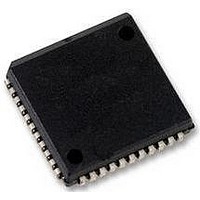
SC16C2550BIA44 NXP Semiconductors, SC16C2550BIA44 Datasheet - Page 9

SC16C2550BIA44
Manufacturer Part Number
SC16C2550BIA44
Description
UART, 2 CH, 16BYTE FIFO, 16C2550
Manufacturer
NXP Semiconductors
Datasheet
1.SC16C2550BIA44518.pdf
(43 pages)
Specifications of SC16C2550BIA44
Data Rate
5Mbps
Transmit Fifo
16Byte
Receive Fifo
16Byte
Transmitter And Receiver Fifo Counter
Yes
Package Type
PLCC
Operating Supply Voltage (max)
5.5V
Mounting
Surface Mount
Pin Count
44
Operating Temperature (min)
-40C
Operating Temperature (max)
85C
Operating Temperature Classification
Industrial
Number Of Channels
2
No. Of Channels
2
Supply Voltage Range
2.25V To 5.5V
Operating Temperature Range
-40°C To +85°C
Digital Ic Case Style
PLCC
No. Of Pins
44
Svhc
No SVHC (18-Jun-2010)
Operating
RoHS Compliant
Uart Features
Independent Transmit & Receive UART Control, Software Selectable Baud Rate Generator
Rohs Compliant
Yes
Lead Free Status / RoHS Status
Compliant
Available stocks
Company
Part Number
Manufacturer
Quantity
Price
Company:
Part Number:
SC16C2550BIA44
Manufacturer:
EVERLIGHT
Quantity:
99
Part Number:
SC16C2550BIA44
Manufacturer:
NXP/恩智浦
Quantity:
20 000
Company:
Part Number:
SC16C2550BIA44,512
Manufacturer:
NXP Semiconductors
Quantity:
10 000
Company:
Part Number:
SC16C2550BIA44,518
Manufacturer:
NXP Semiconductors
Quantity:
10 000
Company:
Part Number:
SC16C2550BIA44,529
Manufacturer:
NXP Semiconductors
Quantity:
10 000
Company:
Part Number:
SC16C2550BIA44518
Manufacturer:
NXP Semiconductors
Quantity:
135
NXP Semiconductors
6. Functional description
SC16C2550B_5
Product data sheet
6.1 UART A-B functions
The SC16C2550B provides serial asynchronous receive data synchronization,
parallel-to-serial and serial-to-parallel data conversions for both the transmitter and
receiver sections. These functions are necessary for converting the serial data stream into
parallel data that is required with digital data systems. Synchronization for the serial data
stream is accomplished by adding start and stop bits to the transmit data to form a data
character (character orientated protocol). Data integrity is insured by attaching a parity bit
to the data character. The parity bit is checked by the receiver for any transmission bit
errors. The electronic circuitry to provide all these functions is fairly complex, especially
when manufactured on a single integrated silicon chip. The SC16C2550B represents such
an integration with greatly enhanced features. The SC16C2550B is fabricated with an
advanced CMOS process.
The SC16C2550B is an upward solution that provides a dual UART capability with
16 bytes of transmit and receive FIFO memory, instead of none in the 16C2450. The
SC16C2550B is designed to work with high speed modems and shared network
environments that require fast data processing time. Increased performance is realized in
the SC16C2550B by the transmit and receive FIFOs. This allows the external processor to
handle more networking tasks within a given time. For example, the ST16C2450 without a
receive FIFO, will require unloading of the RHR in 93 microseconds (this example uses a
character length of 11 bits, including start/stop bits at 115.2 kbit/s). This means the
external CPU will have to service the receive FIFO less than every 100 microseconds.
However, with the 16-byte FIFO in the SC16C2550B, the data buffer will not require
unloading/loading for 1.53 ms. This increases the service interval, giving the external CPU
additional time for other applications and reducing the overall UART interrupt servicing
time. In addition, the four selectable receive FIFO trigger interrupt levels are uniquely
provided for maximum data throughput performance especially when operating in a
multi-channel environment. The FIFO memory greatly reduces the bandwidth requirement
of the external controlling CPU, increases performance and reduces power consumption.
The SC16C2550B is capable of operation up to 5 Mbit/s with a 80 MHz clock. With a
crystal or external clock input of 7.3728 MHz, the user can select data rates up to
460.8 kbit/s.
The rich feature set of the SC16C2550B is available through internal registers. Selectable
receive FIFO trigger levels, selectable TX and RX baud rates and modem interface
controls are all standard features. Following a power-on reset or an external reset, the
SC16C2550B is software compatible with the previous generation, ST16C2450.
The UART provides the user with the capability to bidirectionally transfer information
between an external CPU, the SC16C2550B package and an external serial device. A
logic 0 on chip select pins CSA and/or CSB allows the user to configure, send data,
and/or receive data via UART channels A through B. Individual channel select functions
are shown in
Table
5 V, 3.3 V and 2.5 V dual UART, 5 Mbit/s (max.), with 16-byte FIFOs
4.
Rev. 05 — 12 January 2009
SC16C2550B
© NXP B.V. 2009. All rights reserved.
9 of 43


