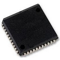
SC16C2550BIA44 NXP Semiconductors, SC16C2550BIA44 Datasheet - Page 18

SC16C2550BIA44
Manufacturer Part Number
SC16C2550BIA44
Description
UART, 2 CH, 16BYTE FIFO, 16C2550
Manufacturer
NXP Semiconductors
Datasheet
1.SC16C2550BIA44518.pdf
(43 pages)
Specifications of SC16C2550BIA44
Data Rate
5Mbps
Transmit Fifo
16Byte
Receive Fifo
16Byte
Transmitter And Receiver Fifo Counter
Yes
Package Type
PLCC
Operating Supply Voltage (max)
5.5V
Mounting
Surface Mount
Pin Count
44
Operating Temperature (min)
-40C
Operating Temperature (max)
85C
Operating Temperature Classification
Industrial
Number Of Channels
2
No. Of Channels
2
Supply Voltage Range
2.25V To 5.5V
Operating Temperature Range
-40°C To +85°C
Digital Ic Case Style
PLCC
No. Of Pins
44
Svhc
No SVHC (18-Jun-2010)
Operating
RoHS Compliant
Uart Features
Independent Transmit & Receive UART Control, Software Selectable Baud Rate Generator
Rohs Compliant
Yes
Lead Free Status / RoHS Status
Compliant
Available stocks
Company
Part Number
Manufacturer
Quantity
Price
Company:
Part Number:
SC16C2550BIA44
Manufacturer:
EVERLIGHT
Quantity:
99
Part Number:
SC16C2550BIA44
Manufacturer:
NXP/恩智浦
Quantity:
20 000
Company:
Part Number:
SC16C2550BIA44,512
Manufacturer:
NXP Semiconductors
Quantity:
10 000
Company:
Part Number:
SC16C2550BIA44,518
Manufacturer:
NXP Semiconductors
Quantity:
10 000
Company:
Part Number:
SC16C2550BIA44,529
Manufacturer:
NXP Semiconductors
Quantity:
10 000
Company:
Part Number:
SC16C2550BIA44518
Manufacturer:
NXP Semiconductors
Quantity:
135
NXP Semiconductors
SC16C2550B_5
Product data sheet
7.3.2 FIFO mode
regardless of the programmed level until the FIFO is full. RXRDY on PLCC44 and
LQFP48 packages transitions LOW when the FIFO reaches the trigger level and
transitions HIGH when the FIFO empties.
Table 10.
Bit
7:6
5:4
3
2
Symbol
FCR[7:6]
FCR[5:4]
FCR[3]
FCR[2]
FIFO Control Register bits description
5 V, 3.3 V and 2.5 V dual UART, 5 Mbit/s (max.), with 16-byte FIFOs
Description
RCVR trigger. These bits are used to set the trigger level for the receive
FIFO interrupt.
An interrupt is generated when the number of characters in the FIFO
equals the programmed trigger level. However, the FIFO will continue to be
loaded until it is full. Refer to
Not used; initialized to logic 0.
DMA mode select.
Transmit operation in mode ‘0’: When the SC16C2550B is in the
16C450 mode (FIFOs disabled; FCR[0] = logic 0) or in the FIFO mode
(FIFOs enabled; FCR[0] = logic 1; FCR[3] = logic 0) and when there are no
characters in the transmit FIFO or Transmit Holding Register, the TXRDYn
pin in PLCC44 or LQFP48 packages will be a logic 0. Once active, the
TXRDYn pin will go to a logic 1 after the first character is loaded into the
Transmit Holding Register.
Receive operation in mode ‘0’: When the SC16C2550B is in mode ‘0’
(FCR[0] = logic 0) or in the FIFO mode (FCR[3] = logic 0) and there is at
least one character in the receive FIFO, the RXRDYn pin will be a logic 0.
Once active, the RXRDYn pin on PLCC44 and LQFP48 packages will go
to a logic 1 when there are no more characters in the receiver.
Transmit operation in mode ‘1’: When the SC16C2550B is in FIFO
mode (FCR[0] = logic 1; FCR[3] = logic 1), the TXRDYn pin on PLCC44
and LQFP48 packages will be a logic 1 when the transmit FIFO is
completely full. It will be a logic 0 if one or more FIFO locations are empty.
Receive operation in mode ‘1’: When the SC16C2550B is in FIFO mode
(FCR[0] = logic 1; FCR[3] = logic 1) and the trigger level has been reached
or a Receive Time-out has occurred, the RXRDYn pin on PLCC44 and
LQFP48 packages will go to a logic 0. Once activated, it will go to a logic 1
after there are no more characters in the FIFO.
XMIT FIFO reset.
Rev. 05 — 12 January 2009
logic 0 (or cleared) = normal default condition
logic 1 = RX trigger level
logic 0 = set DMA mode ‘0’
logic 1 = set DMA mode ‘1’
logic 0 = Transmit FIFO not reset (normal default condition).
logic 1 = clears the contents of the transmit FIFO and resets the FIFO
counter logic (the Transmit Shift Register is not cleared or altered). This
bit will return to a logic 0 after clearing the FIFO.
Table
11.
SC16C2550B
© NXP B.V. 2009. All rights reserved.
18 of 43


