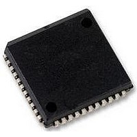
SC16C2550BIA44 NXP Semiconductors, SC16C2550BIA44 Datasheet - Page 6

SC16C2550BIA44
Manufacturer Part Number
SC16C2550BIA44
Description
UART, 2 CH, 16BYTE FIFO, 16C2550
Manufacturer
NXP Semiconductors
Datasheet
1.SC16C2550BIA44518.pdf
(43 pages)
Specifications of SC16C2550BIA44
Data Rate
5Mbps
Transmit Fifo
16Byte
Receive Fifo
16Byte
Transmitter And Receiver Fifo Counter
Yes
Package Type
PLCC
Operating Supply Voltage (max)
5.5V
Mounting
Surface Mount
Pin Count
44
Operating Temperature (min)
-40C
Operating Temperature (max)
85C
Operating Temperature Classification
Industrial
Number Of Channels
2
No. Of Channels
2
Supply Voltage Range
2.25V To 5.5V
Operating Temperature Range
-40°C To +85°C
Digital Ic Case Style
PLCC
No. Of Pins
44
Svhc
No SVHC (18-Jun-2010)
Operating
RoHS Compliant
Uart Features
Independent Transmit & Receive UART Control, Software Selectable Baud Rate Generator
Rohs Compliant
Yes
Lead Free Status / RoHS Status
Compliant
Available stocks
Company
Part Number
Manufacturer
Quantity
Price
Company:
Part Number:
SC16C2550BIA44
Manufacturer:
EVERLIGHT
Quantity:
99
Part Number:
SC16C2550BIA44
Manufacturer:
NXP/恩智浦
Quantity:
20 000
Company:
Part Number:
SC16C2550BIA44,512
Manufacturer:
NXP Semiconductors
Quantity:
10 000
Company:
Part Number:
SC16C2550BIA44,518
Manufacturer:
NXP Semiconductors
Quantity:
10 000
Company:
Part Number:
SC16C2550BIA44,529
Manufacturer:
NXP Semiconductors
Quantity:
10 000
Company:
Part Number:
SC16C2550BIA44518
Manufacturer:
NXP Semiconductors
Quantity:
135
NXP Semiconductors
Table 3.
SC16C2550B_5
Product data sheet
Symbol
A0
A1
A2
CSA
CSB
D0
D1
D2
D3
D4
D5
D6
D7
GND
INTA
INTB
IOR
IOW
OP2A
OP2B
Pin
HVQFN32 DIP40 PLCC44 LQFP48
19
18
17
8
9
27
28
29
30
31
32
1
2
13
21
20
14
12
22
7
Pin description
5.2 Pin description
28
27
26
14
15
1
2
3
4
5
6
7
8
20
30
29
21
18
31
13
31
30
29
16
17
2
3
4
5
6
7
8
9
22
33
32
24
20
35
15
28
27
26
10
11
44
45
46
47
48
1
2
3
17
30
29
19
15
32
9
5 V, 3.3 V and 2.5 V dual UART, 5 Mbit/s (max.), with 16-byte FIFOs
Rev. 05 — 12 January 2009
Type
I
I
I
I
I
I/O
I/O
I/O
I/O
I/O
I/O
I/O
I/O
I
O
O
I
I
O
O
Description
Address 0 select bit. Internal register address selection.
Address 1 select bit. Internal register address selection.
Address 2 select bit. Internal register address selection.
Chip Select A, B (active LOW). This function is associated
with individual channels, A through B. These pins enable data
transfers between the user CPU and the SC16C2550B for the
channel(s) addressed. Individual UART sections (A, B) are
addressed by providing a logic 0 on the respective CSA, CSB
pin.
Data bus (bidirectional). These pins are the 8-bit, 3-state data
bus for transferring information to or from the controlling CPU.
D0 is the least significant bit and the first data bit in a transmit
or receive serial data stream.
Signal and power ground.
Interrupt A, B (3-state). This function is associated with
individual channel interrupts, INTA, INTB. INTA, INTB are
enabled when MCR bit 3 is set to a logic 1, interrupts are
enabled in the Interrupt Enable Register (IER) and is active
when an interrupt condition exists. Interrupt conditions include:
receiver errors, available receiver buffer data, transmit buffer
empty or when a modem status flag is detected.
Read strobe (active LOW strobe). A logic 0 transition on this
pin will load the contents of an internal register defined by
address bits A0 to A2 onto the SC16C2550B data bus
(D0 to D7) for access by external CPU.
Write strobe (active LOW strobe). A logic 0 transition on this
pin will transfer the contents of the data bus (D0 to D7) from the
external CPU to an internal register that is defined by address
bits A0 to A2.
Output 2 (user-defined). This function is associated with
individual channels, A through B. The state at these pin(s) are
defined by the user and through MCR register bit 3. INTA, INTB
are set to the active mode and OP2 to logic 0 when MCR[3] is
set to a logic 1. INTA, INTB are set to the 3-state mode and
OP2 to a logic 1 when MCR[3] is set to a logic 0. See
“Modem Control Register bits
Since these bits control both the INTA, INTB operation and
OP2 outputs, only one function should be used at one time, INT
or OP2.
description”, bit 3 (MCR[3]).
SC16C2550B
© NXP B.V. 2009. All rights reserved.
Table 18
6 of 43


