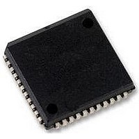
SC16C2550BIA44 NXP Semiconductors, SC16C2550BIA44 Datasheet - Page 25

SC16C2550BIA44
Manufacturer Part Number
SC16C2550BIA44
Description
UART, 2 CH, 16BYTE FIFO, 16C2550
Manufacturer
NXP Semiconductors
Datasheet
1.SC16C2550BIA44518.pdf
(43 pages)
Specifications of SC16C2550BIA44
Data Rate
5Mbps
Transmit Fifo
16Byte
Receive Fifo
16Byte
Transmitter And Receiver Fifo Counter
Yes
Package Type
PLCC
Operating Supply Voltage (max)
5.5V
Mounting
Surface Mount
Pin Count
44
Operating Temperature (min)
-40C
Operating Temperature (max)
85C
Operating Temperature Classification
Industrial
Number Of Channels
2
No. Of Channels
2
Supply Voltage Range
2.25V To 5.5V
Operating Temperature Range
-40°C To +85°C
Digital Ic Case Style
PLCC
No. Of Pins
44
Svhc
No SVHC (18-Jun-2010)
Operating
RoHS Compliant
Uart Features
Independent Transmit & Receive UART Control, Software Selectable Baud Rate Generator
Rohs Compliant
Yes
Lead Free Status / RoHS Status
Compliant
Available stocks
Company
Part Number
Manufacturer
Quantity
Price
Company:
Part Number:
SC16C2550BIA44
Manufacturer:
EVERLIGHT
Quantity:
99
Part Number:
SC16C2550BIA44
Manufacturer:
NXP/恩智浦
Quantity:
20 000
Company:
Part Number:
SC16C2550BIA44,512
Manufacturer:
NXP Semiconductors
Quantity:
10 000
Company:
Part Number:
SC16C2550BIA44,518
Manufacturer:
NXP Semiconductors
Quantity:
10 000
Company:
Part Number:
SC16C2550BIA44,529
Manufacturer:
NXP Semiconductors
Quantity:
10 000
Company:
Part Number:
SC16C2550BIA44518
Manufacturer:
NXP Semiconductors
Quantity:
135
NXP Semiconductors
8. Limiting values
Table 23.
In accordance with the Absolute Maximum Rating System (IEC 60134).
9. Static characteristics
Table 24.
T
[1]
SC16C2550B_5
Product data sheet
Symbol
V
V
T
T
P
Symbol Parameter
V
V
V
V
V
V
I
I
I
C
LIL
L(clk)
CC
amb
amb
stg
CC
n
tot
IL(clk)
IH(clk)
IL
IH
OL
OH
i
/pack
Except XTAL2, V
= 40 C to +85 C; tolerance of V
clock LOW-level input voltage
clock HIGH-level input voltage
LOW-level input voltage
HIGH-level input voltage
LOW-level output voltage
HIGH-level output voltage
LOW-level input leakage current
clock leakage current
supply current
input capacitance
Limiting values
Static characteristics
Parameter
supply voltage
voltage on any other pin
operating temperature
storage temperature
total power dissipation per package
OL
= 1 V typical.
CC
10 %; unless otherwise specified.
Conditions
except X1 clock
except X1 clock
on all outputs
I
(data bus)
I
(other outputs)
I
(data bus)
I
(other outputs)
f = 5 MHz
OH
OH
OH
OH
5 V, 3.3 V and 2.5 V dual UART, 5 Mbit/s (max.), with 16-byte FIFOs
I
(data bus)
I
(other outputs)
I
(data bus)
I
(other outputs)
OL
OL
OL
OL
= 5 mA
= 1 mA
= 800 A
= 400 A
Rev. 05 — 12 January 2009
= 5 mA
= 4 mA
= 2 mA
= 1.6 mA
Conditions
at D7 to D0 pins
at input only pins
[1]
1.85
1.85
Min
V
1.8
1.6
0.3
0.3
-
-
-
-
-
-
-
-
-
-
CC
= 2.5 V
+0.45
+0.65
Max
V
0.4
0.4
3.5
10
30
5
CC
-
-
-
-
-
-
-
Min
-
GND
GND
-
40
65
Min
V
2.4
2.0
2.0
0.3
0.3
-
-
-
-
-
-
-
-
-
-
-
CC
0.3
0.3
= 3.3 V
SC16C2550B
Max
+0.6
+0.8
V
0.4
4.5
10
30
5
CC
-
-
-
-
-
-
-
-
Max
7
V
5.3
+85
+150
500
CC
+ 0.3
Min
V
© NXP B.V. 2009. All rights reserved.
3.0
2.2
2.4
0.5
0.5
-
-
-
-
-
-
-
-
-
-
-
CC
= 5.0 V
Max
+0.6
+0.8
V
0.4
4.5
10
30
5
CC
-
-
-
-
-
-
-
-
Unit
V
V
V
mW
C
C
25 of 43
Unit
V
V
V
V
V
V
V
V
V
V
V
V
mA
pF
A
A


