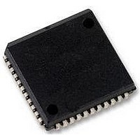
SC16C2550BIA44 NXP Semiconductors, SC16C2550BIA44 Datasheet - Page 11

SC16C2550BIA44
Manufacturer Part Number
SC16C2550BIA44
Description
UART, 2 CH, 16BYTE FIFO, 16C2550
Manufacturer
NXP Semiconductors
Datasheet
1.SC16C2550BIA44518.pdf
(43 pages)
Specifications of SC16C2550BIA44
Data Rate
5Mbps
Transmit Fifo
16Byte
Receive Fifo
16Byte
Transmitter And Receiver Fifo Counter
Yes
Package Type
PLCC
Operating Supply Voltage (max)
5.5V
Mounting
Surface Mount
Pin Count
44
Operating Temperature (min)
-40C
Operating Temperature (max)
85C
Operating Temperature Classification
Industrial
Number Of Channels
2
No. Of Channels
2
Supply Voltage Range
2.25V To 5.5V
Operating Temperature Range
-40°C To +85°C
Digital Ic Case Style
PLCC
No. Of Pins
44
Svhc
No SVHC (18-Jun-2010)
Operating
RoHS Compliant
Uart Features
Independent Transmit & Receive UART Control, Software Selectable Baud Rate Generator
Rohs Compliant
Yes
Lead Free Status / RoHS Status
Compliant
Available stocks
Company
Part Number
Manufacturer
Quantity
Price
Company:
Part Number:
SC16C2550BIA44
Manufacturer:
EVERLIGHT
Quantity:
99
Part Number:
SC16C2550BIA44
Manufacturer:
NXP/恩智浦
Quantity:
20 000
Company:
Part Number:
SC16C2550BIA44,512
Manufacturer:
NXP Semiconductors
Quantity:
10 000
Company:
Part Number:
SC16C2550BIA44,518
Manufacturer:
NXP Semiconductors
Quantity:
10 000
Company:
Part Number:
SC16C2550BIA44,529
Manufacturer:
NXP Semiconductors
Quantity:
10 000
Company:
Part Number:
SC16C2550BIA44518
Manufacturer:
NXP Semiconductors
Quantity:
135
NXP Semiconductors
SC16C2550B_5
Product data sheet
6.3 FIFO operation
6.4 Hardware/software and time-out interrupts
The 16-byte transmit and receive data FIFOs are enabled by the FIFO Control Register
(FCR) bit 0. The user can set the receive trigger level via FCR bits 7:6, but not the transmit
trigger level. The receiver FIFO section includes a time-out function to ensure data is
delivered to the external CPU. An interrupt is generated whenever the Receive Holding
Register (RHR) has not been read following the loading of a character or the receive
trigger level has not been reached.
Table 6.
The interrupts are enabled by IER[3:0]. Care must be taken when handling these
interrupts. Following a reset, if Interrupt Enable Register (IER) bit 1 = 1, the SC16C2550B
will issue a Transmit Holding Register interrupt. This interrupt must be serviced prior to
continuing operations. The ISR register provides the current singular highest priority
interrupt only. A condition can exist where a higher priority interrupt may mask the lower
priority interrupt(s). Only after servicing the higher pending interrupt will the lower priority
interrupt(s) be reflected in the status register. Servicing the interrupt without investigating
further interrupt conditions can result in data errors.
When two interrupt conditions have the same priority, it is important to service these
interrupts correctly. Receive Data Ready and Receive Time Out have the same interrupt
priority (when enabled by IER[0]). The receiver issues an interrupt after the number of
characters have reached the programmed trigger level. In this case, the SC16C2550B
FIFO may hold more characters than the programmed trigger level. Following the removal
of a data byte, the user should re-check LSR[0] for additional characters. A Receive Time
Out will not occur if the receive FIFO is empty. The time-out counter is reset at the center
of each stop bit received or each time the Receive Holding Register (RHR) is read. The
actual time-out value is 4 character time, including data information length, start bit, parity
bit and the size of stop bit, that is, 1 , 1.5 or 2 bit times.
Selected trigger level (characters)
1
4
8
14
Flow control mechanism
5 V, 3.3 V and 2.5 V dual UART, 5 Mbit/s (max.), with 16-byte FIFOs
Rev. 05 — 12 January 2009
INTn pin activation
1
4
8
14
SC16C2550B
© NXP B.V. 2009. All rights reserved.
11 of 43


