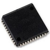
SC16C2550BIA44 NXP Semiconductors, SC16C2550BIA44 Datasheet - Page 23

SC16C2550BIA44
Manufacturer Part Number
SC16C2550BIA44
Description
UART, 2 CH, 16BYTE FIFO, 16C2550
Manufacturer
NXP Semiconductors
Datasheet
1.SC16C2550BIA44518.pdf
(43 pages)
Specifications of SC16C2550BIA44
Data Rate
5Mbps
Transmit Fifo
16Byte
Receive Fifo
16Byte
Transmitter And Receiver Fifo Counter
Yes
Package Type
PLCC
Operating Supply Voltage (max)
5.5V
Mounting
Surface Mount
Pin Count
44
Operating Temperature (min)
-40C
Operating Temperature (max)
85C
Operating Temperature Classification
Industrial
Number Of Channels
2
No. Of Channels
2
Supply Voltage Range
2.25V To 5.5V
Operating Temperature Range
-40°C To +85°C
Digital Ic Case Style
PLCC
No. Of Pins
44
Svhc
No SVHC (18-Jun-2010)
Operating
RoHS Compliant
Uart Features
Independent Transmit & Receive UART Control, Software Selectable Baud Rate Generator
Rohs Compliant
Yes
Lead Free Status / RoHS Status
Compliant
Available stocks
Company
Part Number
Manufacturer
Quantity
Price
Company:
Part Number:
SC16C2550BIA44
Manufacturer:
EVERLIGHT
Quantity:
99
Part Number:
SC16C2550BIA44
Manufacturer:
NXP/恩智浦
Quantity:
20 000
Company:
Part Number:
SC16C2550BIA44,512
Manufacturer:
NXP Semiconductors
Quantity:
10 000
Company:
Part Number:
SC16C2550BIA44,518
Manufacturer:
NXP Semiconductors
Quantity:
10 000
Company:
Part Number:
SC16C2550BIA44,529
Manufacturer:
NXP Semiconductors
Quantity:
10 000
Company:
Part Number:
SC16C2550BIA44518
Manufacturer:
NXP Semiconductors
Quantity:
135
NXP Semiconductors
SC16C2550B_5
Product data sheet
7.8 Modem Status Register (MSR)
Table 19.
This register provides the current state of the control interface signals from the modem or
other peripheral device to which the SC16C2550B is connected. Four bits of this register
are used to indicate the changed information. These bits are set to a logic 1 whenever a
control input from the modem changes state. These bits are set to a logic 0 whenever the
CPU reads this register.
Table 20.
[1]
Bit
0
Bit
7
6
5
4
3
2
1
0
Whenever any MSR bit 3:0 is set to logic 1, a Modem Status Interrupt will be generated.
Symbol
LSR[0]
Symbol
MSR[7]
MSR[6]
MSR[5]
MSR[4]
MSR[3]
MSR[2]
MSR[1]
MSR[0]
Line Status Register bits description
Modem Status Register bits description
Description
Receive data ready.
logic 0 = no data in Receive Holding Register or FIFO (normal default
condition)
logic 1 = data has been received and is saved in the Receive Holding Register
or FIFO
5 V, 3.3 V and 2.5 V dual UART, 5 Mbit/s (max.), with 16-byte FIFOs
Description
CD. During normal operation, this bit is the complement of the CD input.
Reading this bit in the Loopback mode produces the state of MCR[3] (OP2).
RI. During normal operation, this bit is the complement of the RI input.
Reading this bit in the Loopback mode produces the state of MCR[2] (OP1).
DSR. During normal operation, this bit is the complement of the DSR input.
During the Loopback mode, this bit is equivalent to MCR[0] (DTR).
CTS. During normal operation, this bit is the complement of the CTS input.
During the Loopback mode, this bit is equivalent to MCR[1] (RTS).
CD
RI
DSR
CTS
logic 0 = no CD change (normal default condition)
logic 1 = the CD input to the SC16C2550B has changed state since the
last time it was read. A modem Status Interrupt will be generated.
logic 0 = no RI change (normal default condition)
logic 1 = the RI input to the SC16C2550B has changed from a logic 0 to a
logic 1. A modem Status Interrupt will be generated.
logic 0 = no DSR change (normal default condition)
logic 1 = the DSR input to the SC16C2550B has changed state since the
last time it was read. A modem Status Interrupt will be generated.
logic 0 = no CTS change (normal default condition)
logic 1 = the CTS input to the SC16C2550B has changed state since the
last time it was read. A modem Status Interrupt will be generated.
Rev. 05 — 12 January 2009
[1]
[1]
[1]
[1]
…continued
SC16C2550B
© NXP B.V. 2009. All rights reserved.
23 of 43


