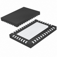
LTC2494IUHF#PBF Linear Technology, LTC2494IUHF#PBF Datasheet - Page 10

LTC2494IUHF#PBF
Manufacturer Part Number
LTC2494IUHF#PBF
Description
IC ADC 16BIT W/PGA 38-QFN
Manufacturer
Linear Technology
Datasheet
1.LTC2494CUHFPBF.pdf
(38 pages)
Specifications of LTC2494IUHF#PBF
Number Of Bits
16
Sampling Rate (per Second)
15
Data Interface
MICROWIRE™, Serial, SPI™
Number Of Converters
1
Power Dissipation (max)
480µW
Voltage Supply Source
Single Supply
Operating Temperature
-40°C ~ 85°C
Mounting Type
Surface Mount
Package / Case
38-WFQFN, Exposed Pad
Lead Free Status / RoHS Status
Lead free / RoHS Compliant
Available stocks
Company
Part Number
Manufacturer
Quantity
Price
pin Functions
LTC2494
typical perForMance characteristics
GND (Pins 1, 3, 4, 5, 6, 31, 32, 33): Ground. Multiple
ground pins internally connected for optimum ground cur-
rent flow and V
pins to a common ground plane through a low impedance
connection. All eight pins must be connected to ground
for proper operation.
NC (Pin 2): No Connection. This pin can be left floating
or tied to GND.
COM (Pin 7): The Common Negative Input (IN
Single-Ended Multiplexer Configurations. The voltage on
CH0 to CH15 and COM pins can have any value between
GND – 0.3V to V
selected inputs (IN
V
Outside this input range, the converter produces unique
overrange and underrange output codes.
CH0 to CH15 (Pins 8 to 23): Analog Inputs. May be pro-
grammed for single-ended or differential mode.
MUXOUTP (Pin 24): Positive Multiplexer Output. Used
to drive an external buffer/amplifier or can be shorted
directly to ADCINP .
0
IN
= (IN
+
– IN
–
CC
) from –0.5 • V
–100
–120
–140
–20
–60
–40
–80
CC
decoupling. Connect each one of these
+
0
and IN
PSRR vs Frequency at V
(2x Speed Mode)
0
+ 0.3V. Within these limits, the two
V
REF
REF
IN
IN
f
T
O
A
CC
+
–
20
= GND
= 25°C
+
–
= GND
= GND
= 4.1V DC ±1.4V
= 2.5V
= GND
40 60
–
) provide a bipolar input range
FREQUENCY AT V
REF
80
/Gain to 0.5 • V
100
120
140
CC
(Hz)
160
CC
180
200
2494 G37
REF
–
) for All
220
/Gain.
ADCINP (Pin 25): Positive ADC Input. Tie to the output
of a buffer/amplifier driven by MUXOUTP or tie directly
to MUXOUTP .
ADCINN (Pin 26): Negative ADC Input. Tie to the output
of a buffer/amplifier driven by MUXOUTN or tie directly
to MUXOUTN.
MUXOUTN (Pin 27): Negative Multiplexer Output. Used
to drive an external buffer/amplifier or can be shorted
directly to ADCINN.
V
a 10µF tantalum capacitor in parallel with a 0.1µF ceramic
capacitor as close to the part as possible.
REF
The voltage on these pins can have any value between
GND and V
remains more positive than the negative reference input,
REF
– REF
• V
on-chip temperature measurement, the minimum value
of REF = 2V.
CC
REF
(Pin 28): Positive Supply Voltage. Bypass to GND with
–
+
, by at least 0.1V. The differential voltage V
(Pin 29), REF
–
/Gain) for all input channels. When performing an
–100
–120
–140
) sets the full-scale range (–0.5 • V
–20
–40
–60
–80
30600
0
CC
PSRR vs Frequency at V
(2x Speed Mode)
V
REF
REF
IN
IN
f
T
O
A
CC
+
–
= GND
as long as the reference positive input, REF
= 25°C
+
–
= GND
= GND
= 4.1V DC ±0.7V
= 2.5V
= GND
30650
FREQUENCY AT V
–
(Pin 30): Differential Reference Input.
30700
CC
(Hz)
30750
CC
2494 G38
30800
REF
/Gain to 0.5
REF
= (REF
2494fd
+
+
,


