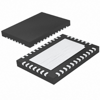
LTC2494IUHF#PBF Linear Technology, LTC2494IUHF#PBF Datasheet - Page 26

LTC2494IUHF#PBF
Manufacturer Part Number
LTC2494IUHF#PBF
Description
IC ADC 16BIT W/PGA 38-QFN
Manufacturer
Linear Technology
Datasheet
1.LTC2494CUHFPBF.pdf
(38 pages)
Specifications of LTC2494IUHF#PBF
Number Of Bits
16
Sampling Rate (per Second)
15
Data Interface
MICROWIRE™, Serial, SPI™
Number Of Converters
1
Power Dissipation (max)
480µW
Voltage Supply Source
Single Supply
Operating Temperature
-40°C ~ 85°C
Mounting Type
Surface Mount
Package / Case
38-WFQFN, Exposed Pad
Lead Free Status / RoHS Status
Lead free / RoHS Compliant
Available stocks
Company
Part Number
Manufacturer
Quantity
Price
applications inForMation
LTC2494
The serial data output pin (SDO) is Hi-Z as long as CS is
HIGH. At any time during the conversion cycle, CS may be
pulled LOW in order to monitor the state of the converter.
Once CS is pulled LOW, SCK goes LOW and EOC is output
to the SDO pin. EOC= 1 while the conversion is in progress
and EOC = 0 if the device is in the sleep state.
When testing EOC, if the conversion is complete (EOC = 0),
the device will exit sleep state. In order to return to the
sleep state and reduce the power consumption, CS must be
pulled HIGH before the device pulls SCK HIGH. When the
device is using its own internal oscillator (f
the first rising edge of SCK occurs 12µs (t
after the falling edge of CS. If f
oscillator of frequency f
If CS remains LOW longer than t
edge of SCK will occur and the conversion result is shifted
out the SDO pin on the falling edge of SCK. The serial
input word (SDI) is shifted into the device on the rising
edge of SCK.
(INTERNAL)
SDO
SCK
SDI
CS
CONVERSION
Figure 10. Internal Serial Clock, Reduced Data Output Length with Valid Channel and Configuration Selection
DON'T CARE
SLEEP
EOSC
<t
EOCTEST
, then t
BIT 23
1
EOC
1
O
is driven by an external
EOCTEST
BIT 22
“0”
EOCTEST
0
2
BIT 21
SIG
EN
10µF
3
, the first rising
EOCTEST
2.7V TO 5.5V
O
= 3.6/f
BIT 20 BIT 19 BIT 18 BIT 17 BIT 16 BIT 15 BIT 14 BIT 13
is tied LOW),
MSB
SGL
4
0.1V TO V
REFERENCE
0.1µF
ANALOG
INPUTS
VOLTAGE
ODD
= 12µs)
5
EOSC
CC
A2
6
.
•
•
•
•
•
•
28
29
30
15
16
23
8
7
V
REF
REF
CH0
CH7
CH8
CH15
COM
A1
CC
•
•
•
•
•
•
7
LTC2494
+
–
DATA INPUT/OUTPUT
After the 24th rising edge of SCK a new conversion au-
tomatically begins. SDO goes HIGH (EOC = 1) and SCK
remains HIGH for the duration of the conversion cycle.
Once the conversion is complete, the cycle repeats.
Typically, CS remains LOW during the data output state.
However, the data output state may be aborted by pull-
ing CS HIGH any time between the 1st rising edge and
the 24th falling edge of SCK (see Figure 10). On the ris-
ing edge of CS, the device aborts the data output state
and immediately initiates a new conversion. In order to
program a new input channel, 8 SCK clock pulses are
required. If the data output sequence is aborted prior to
the 8th falling edge of SCK, the new input data is ignored
and the previously selected input channel remains valid.
If the rising edge of CS occurs after the 8th falling edge
of SCK, the new input channel is loaded and valid for the
next conversion cycle. If CS goes HIGH between the 8th
falling edge and the 16th falling edge of SCK, the new
channel is still loaded, but the converter configuration
A0
SDO
GND
8
SCK
SDI
CS
f
O
1,3,4,5,6,31,32,33,39
EN2
34
38
35
37
36
9
IM
10
4-WIRE
SPI INTERFACE
= EXTERNAL OSCILLATOR
= INTERNAL OSCILLATOR
FA
11
BIT 12 BIT 11
FB
12
V
CC
SPD
OPTIONAL
10k
13
BIT 10
GS2
14
BIT 9
GS1
15
BIT 8
GS0
16
BIT 7
DON'T CARE
CONVERSION
Hi-Z
2494fd
2494 F10


