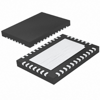
LTC2494IUHF#PBF Linear Technology, LTC2494IUHF#PBF Datasheet - Page 30

LTC2494IUHF#PBF
Manufacturer Part Number
LTC2494IUHF#PBF
Description
IC ADC 16BIT W/PGA 38-QFN
Manufacturer
Linear Technology
Datasheet
1.LTC2494CUHFPBF.pdf
(38 pages)
Specifications of LTC2494IUHF#PBF
Number Of Bits
16
Sampling Rate (per Second)
15
Data Interface
MICROWIRE™, Serial, SPI™
Number Of Converters
1
Power Dissipation (max)
480µW
Voltage Supply Source
Single Supply
Operating Temperature
-40°C ~ 85°C
Mounting Type
Surface Mount
Package / Case
38-WFQFN, Exposed Pad
Lead Free Status / RoHS Status
Lead free / RoHS Compliant
Available stocks
Company
Part Number
Manufacturer
Quantity
Price
applications inForMation
ANALOG
LTC2494
difference between V
common mode voltage of 2.5V and an input common mode
of 1.5V, the common mode input current is approximately
0.74µA (in simultaneous 50Hz/60Hz rejection mode). This
common mode input current does not degrade the accuracy
if the source impedances tied to IN
Mismatches in source impedance lead to a fixed offset
error but do not effect the linearity or full-scale reading.
A 1% mismatch in a 1k source resistance leads to a 74µV
shift in offset voltage.
In applications where the common mode input voltage
varies as a function of the input signal level (single-ended
type sensors), the common mode input current varies
proportionally with input voltage. For the case of balanced
input impedances, the common mode input current effects
are rejected by the large CMRR of the LTC2494, leading
to little degradation in accuracy. Mismatches in source
impedances lead to gain errors proportional to the dif-
ference between the common mode input and common
mode reference. 1% mismatches in 1k source resistances
lead to gain errors on the order of 15ppm. Based on the
stability of the internal sampling capacitors and the ac-
curacy of the internal oscillator, a one-time calibration will
remove this error.
INPUTS
0
Figure 13. External Buffers Provide High Impedance Inputs and
17
INPUT
Amplifier Offsets are Automatically Cancelled.
MUX
3
2
6
5
–
–
+
+
1/2 LTC6078
1/2 LTC6078
IN(CM)
LTC2494
and V
1
7
REF(CM)
+
1k
1k
and IN
. For a reference
EASY DRIVE
–
INPUTS
WITH
are matched.
2494 F13
ADC
0.1µF
0.1µF
SDO
SCK
SDI
CS
In addition to the input sampling current, the input ESD
protection diodes have a temperature dependent leakage
current. This current, nominally 1nA (±10nA max) results
in a small offset shift. A 1k source resistance will create a
1µV typical and a 10µV maximum offset voltage.
Automatic Offset Calibration of External Buffers/
Amplifiers
In addition to the Easy Drive input current cancellation,
the LTC2494 enables an external amplifier to be inserted
between the multiplexer output and the ADC input (see
Figure 13). This is useful in applications where balanced
source impedances are not possible. One pair of external
buffers/amplifiers can be shared between all 17 analog
inputs. The LTC2494 performs an internal offset calibration
every conversion cycle in order to remove the offset and
drift of the ADC. This calibration is performed through a
combination of front end switching and digital process-
ing. Since the external amplifier is placed between the
multiplexer and the ADC, it is inside this correction loop.
This results in automatic offset correction and offset drift
removal of the external amplifier.
The LTC6078 is an excellent amplifier for this function.
It operates with supply voltages as low as 2.7V and its
noise level is 18nV/√Hz. The Easy Drive input technology
of the LTC2494 enables an RC network to be added directly
to the output of the LTC6078. The capacitor reduces the
magnitude of the current spikes seen at the input to the
ADC and the resistor isolates the capacitor load from the
op-amp output enabling stable operation.
Reference Current
Similar to the analog inputs, the LTC2494 samples the
differential reference pins (REF
small amounts of charge to and from these pins, thus
producing a dynamic reference current. If incomplete set-
tling occurs (as a function the reference source resistance
and reference bypass capacitance) linearity and gain errors
are introduced.
For relatively small values of external reference capaci-
tance (C
settles for reference impedances of many kΩ (if C
REF
< 1nF), the voltage on the sampling capacitor
+
and REF
–
) transferring
REF
2494fd
=


