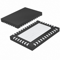
LTC2494IUHF#PBF Linear Technology, LTC2494IUHF#PBF Datasheet - Page 28

LTC2494IUHF#PBF
Manufacturer Part Number
LTC2494IUHF#PBF
Description
IC ADC 16BIT W/PGA 38-QFN
Manufacturer
Linear Technology
Datasheet
1.LTC2494CUHFPBF.pdf
(38 pages)
Specifications of LTC2494IUHF#PBF
Number Of Bits
16
Sampling Rate (per Second)
15
Data Interface
MICROWIRE™, Serial, SPI™
Number Of Converters
1
Power Dissipation (max)
480µW
Voltage Supply Source
Single Supply
Operating Temperature
-40°C ~ 85°C
Mounting Type
Surface Mount
Package / Case
38-WFQFN, Exposed Pad
Lead Free Status / RoHS Status
Lead free / RoHS Compliant
Available stocks
Company
Part Number
Manufacturer
Quantity
Price
applications inForMation
LTC2494
Whenever SCK is LOW, the LTC2494’s internal pull-up at
SCK is disabled. Normally, SCK is not externally driven if
the device is operating in the internal SCK timing mode.
However, certain applications may require an external
driver on SCK. If the driver goes Hi-Z after outputting a
LOW signal, the internal pull-up is disabled. An external
10k pull-up resistor prevents the device from exiting the
internal SCK mode under this condition.
A similar situation may occur during the sleep state when
CS is pulsed HIGH-LOW-HIGH in order to test the conver-
sion status. If the device is in the sleep state (EOC = 0),
SCK will go LOW. If CS goes HIGH before the time t
the internal pull-up is activated. If SCK is heavily loaded,
the internal pull-up may not restore SCK to a HIGH state
before the next falling edge of CS. The external 10k pull-up
resistor prevents the device from exiting the internal SCK
mode under this condition.
PRESERVING THE CONVERTER ACCURACY
The LTC2494 is designed to reduce as much as possible
sensitivity to device decoupling, PCB layout, anti-aliasing
circuits, line frequency perturbations and temperature
sensitivity. In order to achieve maximum performance a
few simple precautions should be observed.
Digital Signal Levels
The LTC2494’s digital interface is easy to use. Its digital
inputs SDI, f
accept standard CMOS logic levels. Internal hysteresis
circuits can tolerate edge transition times as slow as
100µs.
The digital input signal range is 0.5V to V
transitions, the CMOS input circuits draw dynamic cur-
rent. For optimal performance, application of signals to
the serial data interface should be reserved for the sleep
and data output periods.
During the conversion period, overshoot and undershoot
of fast digital signals applied to both the serial digital
interface and the external oscillator pin (f
the converter performance. Undershoot and overshoot
occur due to impedance mismatch of the circuit board
trace at the converter pin when the transition time of an
O
, CS and SCK (in external serial clock mode)
CC
O
) may degrade
– 0.5V. During
EOCtest
,
external control signal is less than twice the propagation
delay from the driver to the input pin. For reference, on a
regular FR-4 board, the propagation delay is approximately
183ps/inch. In order to prevent overshoot, a driver with
a 1ns transition time must be connected to the converter
through a trace shorter than 2.5 inches. This becomes
difficult when shared control lines are used and multiple
reflections occur.
Parallel termination near the input pin of the LTC2494 will
eliminate this problem, but will increase the driver power
dissipation. A series resistor from 27Ω to 54Ω (depend-
ing on the trace impedance and connection) placed near
the driver will also eliminate over/under shoot without
additional driver power dissipation.
For many applications, the serial interface pins (SCK, SDI,
CS, f
degradation occurs. On the other hand, if an external
oscillator is used (f
the conversion cycle. Moreover, the digital filter rejection
is minimal at the clock rate applied to f
taken to ensure external inputs and reference lines do not
cross this signal or run near it. These issues are avoided
when using the internal oscillator.
Driving the Input and Reference
The input and reference pins of the LTC2494 are connected
directly to a switched capacitor network. Depending on
the relationship between the differential input voltage and
the differential reference voltage, these capacitors are
switched between these four pins. Each time a capacitor
is switched between two of these pins, a small amount
of charge is transferred. A simplified equivalent circuit is
shown in Figure 12.
When using the LTC2494’s internal oscillator, the input
capacitor array is switched at 123kHz. The effect of the
charge transfer depends on the circuitry driving the in-
put/reference pins. If the total external RC time constant
is less then 580ns the errors introduced by the sampling
process are negligible since complete settling occurs.
Typically, the reference inputs are driven from a low imped-
ance source. In this case, complete settling occurs even
with large external bypass capacitors. The inputs (CH0 to
CH15, COM), on the other hand, are typically driven from
O
) remain static during the conversion cycle and no
O
driven externally) it is active during
O
. Care must be
2494fd


