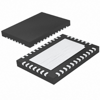
LTC2494IUHF#PBF Linear Technology, LTC2494IUHF#PBF Datasheet - Page 18

LTC2494IUHF#PBF
Manufacturer Part Number
LTC2494IUHF#PBF
Description
IC ADC 16BIT W/PGA 38-QFN
Manufacturer
Linear Technology
Datasheet
1.LTC2494CUHFPBF.pdf
(38 pages)
Specifications of LTC2494IUHF#PBF
Number Of Bits
16
Sampling Rate (per Second)
15
Data Interface
MICROWIRE™, Serial, SPI™
Number Of Converters
1
Power Dissipation (max)
480µW
Voltage Supply Source
Single Supply
Operating Temperature
-40°C ~ 85°C
Mounting Type
Surface Mount
Package / Case
38-WFQFN, Exposed Pad
Lead Free Status / RoHS Status
Lead free / RoHS Compliant
Available stocks
Company
Part Number
Manufacturer
Quantity
Price
applications inForMation
LTC2494
INPUT DATA FORMAT
The LTC2494 serial input word is 16 bits long and contains
two distinct sets of data. The first set (SGL, ODD, A2, A1,
A0) is used to select the input channel. The second set of
data (IM, FA, FB, SPD, GS2, GS1, GS0) is used to select
the frequency rejection, speed mode (1x, 2x), temperature
measurement and gain.
After power-up, the device initiates an internal reset cycle
which sets the input channel to CH0 – CH1 (IN
CH1), the frequency rejection to simultaneous 50Hz/60Hz,
1x output rate (auto-calibration enabled), and gain = 1. The
first conversion automatically begins at power-up using this
default configuration. Once the conversion is complete, a
new word may be written into the device.
The first three bits shifted into the device consist of two
preamble bits and an enable bit. These bits are used to
enable the device configuration and input channel selec-
tion. Valid settings for these three bits are 000, 100 and
101. Other combinations should be avoided. If the first
three bits are 000 or 100, the following data is ignored
(don’t care) and the previously selected input channel and
configuration remain valid for the next conversion.
If the first three bits shifted into the device are 101, then
the next five bits select the input channel for the next
conversion cycle (see Table 3).
Table 2. LTC2494 Output Data Format
DIFFERENTIAL INPUT VOLTAGE
V
V
FS** – 1LSB
0.5 • FS**
0.5 • FS** – 1LSB
0
–1LSB
–0.5 • FS**
–0.5 • FS** – 1LSB
–FS**
V
*The differential input voltage V
***The sign bit changes state during the 0 output code when the device is operating in the 2x speed mode.
IN
IN
IN
*
* ≥ FS**
* < –FS**
IN
= IN
BIT 23
EOC
+
0
0
0
0
0
0
0
0
0
0
– IN
–
. **The full-scale voltage FS = 0.5 • V
BIT 22
DMY
0
0
0
0
0
0
0
0
0
0
+
= CH0, IN
1/0***
BIT 21
SIG
1
1
1
1
0
0
0
0
0
–
=
BIT 20
MSB
1
0
0
0
0
1
1
1
1
0
The first input bit following the 101 sequence (SGL) de-
termines if the input selection is differential (SGL = 0) or
single-ended (SGL = 1). For SGL = 0, two adjacent channels
can be selected to form a differential input. For SGL = 1, one
of 16 channels is selected as the positive input. The negative
input is COM for all single-ended operations. The remaining
4 bits (ODD, A2, A1, A0) determine which channel(s) is/are
selected and the polarity (for a differential input).
The next serial input bit immediately following the input
channel selection is the enable bit for the conversion
configuration (EN2). If this bit is set to 0, then the next
conversion is performed using the previously selected
converter configuration. This is useful in systems using
the same rejection/speed for all input channels and for
backward compatibility with the LTC2418/LTC2414 families
of delta-sigma ADCs.
The second set of configuration data can be loaded into the
device by setting EN2 = 1 (see Table 4). The first bit (IM)
is used to select the internal temperature sensor. If IM = 1,
the following conversion will be performed on the internal
temperature sensor rather than the selected input channel.
The next 2 bits (FA and FB) are used to set the rejection
frequency. The next bit (SPD) is used to select either the
1x output rate if SPD = 0 (auto-calibration is enabled and
the offset is continuously calibrated and removed from
the final conversion result) or the 2x output rate if SPD
BIT 19
0
1
1
0
0
1
1
0
0
1
REF
/Gain.
BIT 18
0
1
0
1
0
1
0
1
0
1
BIT 17
0
1
0
1
0
1
0
1
0
1
…
…
…
…
…
…
…
…
…
…
…
BIT 4
0
1
0
1
0
1
0
1
0
1
BITS 3 TO 0
0000
0000
0000
0000
0000
0000
0000
0000
0000
0000
2494fd


