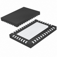
LTC2494IUHF#PBF Linear Technology, LTC2494IUHF#PBF Datasheet - Page 27

LTC2494IUHF#PBF
Manufacturer Part Number
LTC2494IUHF#PBF
Description
IC ADC 16BIT W/PGA 38-QFN
Manufacturer
Linear Technology
Datasheet
1.LTC2494CUHFPBF.pdf
(38 pages)
Specifications of LTC2494IUHF#PBF
Number Of Bits
16
Sampling Rate (per Second)
15
Data Interface
MICROWIRE™, Serial, SPI™
Number Of Converters
1
Power Dissipation (max)
480µW
Voltage Supply Source
Single Supply
Operating Temperature
-40°C ~ 85°C
Mounting Type
Surface Mount
Package / Case
38-WFQFN, Exposed Pad
Lead Free Status / RoHS Status
Lead free / RoHS Compliant
Available stocks
Company
Part Number
Manufacturer
Quantity
Price
applications inForMation
remains unchanged. In order to program both the input
channel and converter configuration, CS must go HIGH
after the 16th falling edge of SCK (at this point all data
has been shifted into the device).
Internal Serial Clock, 3-Wire I/O, Continuous
Conversion.
This timing mode uses a 3-wire interface. The conversion
result is shifted out of the device by an internally generated
serial clock (SCK) signal (see Figure 11). In this case, CS is
permanently tied to ground, simplifying the user interface
or transmission over an isolation barrier.
The internal serial clock mode is selected at the end of the
power-on reset (POR) cycle. The POR cycle is concluded
approximately 4ms after V
pull-up is active during the POR cycle; therefore, the internal
serial clock timing mode is automatically selected if SCK
is floating or driven HIGH.
During the conversion, the SCK and the serial data output
pin (SDO) are HIGH (EOC = 1). Once the conversion is
(INTERNAL)
SDO
SCK
SDI
CS
CONVERSION
DON'T CARE
BIT 23
EOC
CC
1
1
exceeds 2V. An internal weak
BIT 22
“0”
0
2
10µF
BIT 21
SIG
Figure 11. Internal Serial Clock, Continuous Operation
EN
2.7V TO 5.5V
3
BIT 20 BIT 19 BIT 18 BIT 17 BIT 16 BIT 15 BIT 14 BIT 13
MSB
SGL
4
0.1V TO V
REFERENCE
0.1µF
ANALOG
INPUTS
VOLTAGE
ODD
5
CC
•
•
•
•
•
•
28
29
30
15
16
23
A2
8
7
6
V
REF
REF
CH0
CH7
CH8
CH15
COM
CC
•
•
•
•
•
•
LTC2494
+
–
A1
7
SDO
GND
SCK
DATA INPUT/OUTPUT
SDI
CS
A0
f
8
O
complete, SCK and SDO go LOW (EOC = 0) indicating
the conversion has finished and the device has entered
the sleep state. The device remains in the sleep state a
minimum amount of time (1/2 the internal SCK period)
then immediately begins outputting and inputting data.
The input data is shifted through the SDI pin on the ris-
ing edge of SCK (including the first rising edge) and the
output data is shifted out the SDO pin on the falling edge
of SCK. The data input/output cycle is concluded and a
new conversion automatically begins after the 24th rising
edge of SCK. During the next conversion, SCK and SDO
remain HIGH until the conversion is complete.
The Use of a 10k Pull-Up on SCK for Internal SCK
Selection
If CS is pulled HIGH while the converter is driving SCK
LOW, the internal pull-up is not available to restore SCK
to a logic HIGH state if SCK is floating. This will cause the
device to exit the internal SCK mode on the next falling
edge of CS. This can be avoided by adding an external 10k
pull-up resistor to the SCK pin.
1,3,4,5,6,31,32,33,39
34
38
35
37
36
EN2
9
3-WIRE
SPI INTERFACE
IM
10
= EXTERNAL OSCILLATOR
= INTERNAL OSCILLATOR
FA
11
BIT 12 BIT 11
FB
12
V
CC
OPTIONAL
10k
SPD
13
BIT 10
GS2
14
GS1
BIT 9
15
GS0
16
LTC2494
BIT 0
24
DON'T CARE
CONVERSION
2494fd
2494 F11


