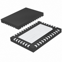
LTC2494IUHF#PBF Linear Technology, LTC2494IUHF#PBF Datasheet - Page 22

LTC2494IUHF#PBF
Manufacturer Part Number
LTC2494IUHF#PBF
Description
IC ADC 16BIT W/PGA 38-QFN
Manufacturer
Linear Technology
Datasheet
1.LTC2494CUHFPBF.pdf
(38 pages)
Specifications of LTC2494IUHF#PBF
Number Of Bits
16
Sampling Rate (per Second)
15
Data Interface
MICROWIRE™, Serial, SPI™
Number Of Converters
1
Power Dissipation (max)
480µW
Voltage Supply Source
Single Supply
Operating Temperature
-40°C ~ 85°C
Mounting Type
Surface Mount
Package / Case
38-WFQFN, Exposed Pad
Lead Free Status / RoHS Status
Lead free / RoHS Compliant
Available stocks
Company
Part Number
Manufacturer
Quantity
Price
applications inForMation
LTC2494
SERIAL INTERFACE TIMING MODES
The LTC2494’s 4-wire interface is SPI and MICROWIRE
compatible. This interface offers several flexible modes
of operation. These include internal/external serial clock,
3- or 4-wire I/O, single cycle or continuous conversion. The
following sections describe each of these timing modes
in detail. In all cases, the converter can use the internal
oscillator (f
the f
format, data output format and performance remain the
same. Refer to Table 6 for a summary.
External Serial Clock, Single Cycle Operation
This timing mode uses an external serial clock to shift out
the conversion result and CS to monitor and control the
state of the conversion cycle (see Figure 6).
The external serial clock mode is selected during the power-
up sequence and on each falling edge of CS. In order to
O
Figure 4. Internal PTAT Digital Output vs Temperature
pin. For each mode, the operating cycle, data input
1020
960
800
640
480
320
160
0
O
0
V
V
SLOPE = 2.45 LSB
= LOW) or an external oscillator connected to
CC
REF
= 5V
= 5V
100
TEMPERATURE (K)
Table 6. LTC2494 Interface Timing Modes
CONFIGURATION
External SCK, Single Cycle
Conversion
External SCK, 3-Wire I/O
Internal SCK, Single Cycle
Conversion
Internal SCK, 3-Wire I/O,
Continuous Conversion
16
/K
200
300
2494 F04
400
SOURCE
External
External
Internal
Internal
SCK
CYCLE CONTROL
CONVERSION
CS and SCK
Continuous
CS↓
SCK
enter and remain in the external SCK mode of operation,
SCK must be driven LOW both at power-up and on each
CS falling edge. If SCK is HIGH on the falling edge of CS,
the device will switch to the internal SCK mode.
The serial data output pin (SDO) is Hi-Z as long as CS is
HIGH. At any time during the conversion cycle, CS may be
pulled LOW in order to monitor the state of the converter.
While CS is LOW, EOC is output to the SDO pin.
EOC = 1 while a conversion is in progress and EOC = 0 if
the conversion is complete and the device is in the sleep
state. Independent of CS, the device automatically enters
the sleep state once the conversion is complete; however,
in order to reduce the power, CS must be HIGH.
When the device is in the sleep state, its conversion result
is held in an internal static shift register. The device remains
in the sleep state until the first rising edge of SCK is seen
while CS is LOW. The input data is then shifted in via the
SDI pin on each rising edge of SCK (including the first rising
DATA OUTPUT
CS and SCK
CONTROL
Internal
–1
–2
–3
–4
–5
SCK
CS↓
Figure 5. Absolute Temperature Error
5
4
3
2
1
0
–55
–30
CONNECTION AND
–5
TEMPERATURE (°C)
WAVEFORMS
Figures 9, 10
Figures 6, 7
Figure 11
Figure 8
20
45
70
95
2494 F05
120
2494fd


