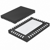
LTC2494IUHF#PBF Linear Technology, LTC2494IUHF#PBF Datasheet - Page 11

LTC2494IUHF#PBF
Manufacturer Part Number
LTC2494IUHF#PBF
Description
IC ADC 16BIT W/PGA 38-QFN
Manufacturer
Linear Technology
Datasheet
1.LTC2494CUHFPBF.pdf
(38 pages)
Specifications of LTC2494IUHF#PBF
Number Of Bits
16
Sampling Rate (per Second)
15
Data Interface
MICROWIRE™, Serial, SPI™
Number Of Converters
1
Power Dissipation (max)
480µW
Voltage Supply Source
Single Supply
Operating Temperature
-40°C ~ 85°C
Mounting Type
Surface Mount
Package / Case
38-WFQFN, Exposed Pad
Lead Free Status / RoHS Status
Lead free / RoHS Compliant
Available stocks
Company
Part Number
Manufacturer
Quantity
Price
pin Functions
SDI (Pin 34): Serial Data Input. This pin is used to select the
gain, line frequency rejection mode, 1x or 2x speed mode,
temperature sensor, as well as the input channel. The serial
data input is applied under control of the serial clock (SCK)
during the data output/input operation. The first conversion
following a new input or mode change is valid.
f
controls the internal conversion clock rate. When f
connected to GND, the converter uses its internal oscil-
lator running at 307.2kHz. The conversion clock may also
be overridden by driving the f
in order to change the output rate and the digital filter
rejection null.
CS (Pin 36): Active LOW Chip Select. A LOW on this pin
enables the digital input/output and wakes up the ADC.
Following each conversion, the ADC automatically enters
the sleep mode and remains in this low power state as
long as CS is HIGH. A LOW-to-HIGH transition on CS
during the data output aborts the data transfer and starts
a new conversion.
O
(Pin 35): Frequency Control Pin. Digital input that
O
pin with an external clock
O
is
SDO (Pin 37): Three-State Digital Output. During the data
output period, this pin is used as the serial data output.
When the chip select pin is HIGH, the SDO pin is in a high
impedance state. During the conversion and sleep periods,
this pin is used as the conversion status output. When
the conversion is in progress this pin is HIGH; once the
conversion is complete SDO goes LOW. The conversion
status is monitored by pulling CS LOW.
SCK (Pin 38): Bidirectional, Digital I/O, Clock Pin. In internal
serial clock operation mode, SCK is generated internally
and is seen as an output on the SCK pin . In external serial
clock operation mode, the digital I/O clock is externally
applied to the SCK pin. The serial clock operation mode
is determined by the logic level applied to the SCK pin at
power-up and during the most recent falling edge of CS.
Exposed Pad (Pin 39): Ground. This pin is ground and
must be soldered to the PCB ground plane. For prototyping
purposes, this pin may remain floating.
LTC2494
2494fd


