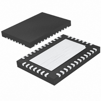
LTC2494IUHF#PBF Linear Technology, LTC2494IUHF#PBF Datasheet - Page 16

LTC2494IUHF#PBF
Manufacturer Part Number
LTC2494IUHF#PBF
Description
IC ADC 16BIT W/PGA 38-QFN
Manufacturer
Linear Technology
Datasheet
1.LTC2494CUHFPBF.pdf
(38 pages)
Specifications of LTC2494IUHF#PBF
Number Of Bits
16
Sampling Rate (per Second)
15
Data Interface
MICROWIRE™, Serial, SPI™
Number Of Converters
1
Power Dissipation (max)
480µW
Voltage Supply Source
Single Supply
Operating Temperature
-40°C ~ 85°C
Mounting Type
Surface Mount
Package / Case
38-WFQFN, Exposed Pad
Lead Free Status / RoHS Status
Lead free / RoHS Compliant
Available stocks
Company
Part Number
Manufacturer
Quantity
Price
applications inForMation
LTC2494
In order to achieve optimum performance, if an external
amplifier is not used, short these pins directly together
(ADCINP to MUXOUTP and ADCINN to MUXOUTN) and
minimize their capacitance to ground.
SERIAL INTERFACE PINS
The LTC2494 transmits the conversion result, reads the
input configuration, and receives a START of conversion
command through a synchronous 3- or 4-wire interface.
During the conversion and sleep states, this interface can be
used to access the converter status. During the data output
state, it is used to read the conversion result, program the
input channel, rejection frequency, speed multiplier, select
the temperature sensor and set the gain.
Serial Clock Input/Output (SCK)
The serial clock pin (SCK) is used to synchronize the data
input/output transfer. Each bit is shifted out of the SDO
pin on the falling edge of SCK and data is shifted into the
SDI pin on the rising edge of SCK.
The serial clock pin (SCK) can be configured as either a
master (SCK is an output generated internally) or a slave
(SCK is an input and applied externally). Master mode
(internal SCK) is selected by simply floating the SCK pin.
Slave mode (external SCK) is selected by driving SCK LOW
during power-up and each falling edge of CS. Specific
details of these SCK modes are described in the Serial
Interface Timing Modes section.
Serial Data Output (SDO)
The serial data output pin (SDO) provides the result of the
last conversion as a serial bit stream (MSB first) during
the data output state. In addition, the SDO pin is used as
an end of conversion indicator during the conversion and
sleep states.
When CS is HIGH, the SDO driver is switched to a high
impedance state in order to share the data output line with
other devices. If CS is brought LOW during the conversion
phase, the EOC bit (SDO pin) will be driven HIGH. Once
the conversion is complete, if CS is brought LOW, EOC will
be driven LOW indicating the conversion is complete and
the result is ready to be shifted out of the device.
Chip Select (CS)
The active LOW CS pin is used to test the conversion status,
enable I/O data transfer, initiate a new conversion, control
the duration of the sleep state and set the SCK mode.
At the conclusion of a conversion cycle, while CS is HIGH,
the device remains in a low power sleep state where the
supply current is reduced several orders of magnitude.
In order to exit the sleep state and enter the data output
state, CS must be pulled LOW. Data is now shifted out
the SDO pin under control of the SCK pin as described
previously.
A new conversion cycle is initiated either at the conclusion
of the data output cycle (all 24 data bits read) or by pulling
CS HIGH any time between the first and 24th rising edges
of the serial clock (SCK). In this case, the data output is
aborted and a new conversion begins.
Serial Data Input (SDI)
The serial data input (SDI) is used to select the input
channel, rejection frequency, speed multiplier, gain, and to
access the integrated temperature sensor. Data is shifted
into the device during the data output/input state on the
rising edge of SCK while CS is LOW.
OUTPUT DATA FORMAT
The LTC2494 serial output stream is 24 bits long. The
first bit indicates the conversion status, the second bit is
always zero, and the third bit conveys sign information.
The next 17 bits are the conversion result, MSB first. The
remaining 4 bits are always LOW.
Bit 23 (first output bit) is the end of conversion (EOC)
indicator. This bit is available on the SDO pin during the
conversion and sleep states whenever CS is LOW. This bit
is HIGH during the conversion cycle, goes LOW once the
conversion is complete, and is Hi-Z when CS is HIGH.
Bit 22 (second output bit) is a dummy bit (DMY) and is
always LOW.
Bit 21 (third output bit) is the conversion result sign
indicator (SIG). If the selected input (V
greater than or equal to 0V, this bit is HIGH. If V
this bit is LOW.
IN
= IN
+
– IN
IN
–
< 0,
2494fd
) is


