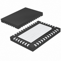
LTC2494IUHF#PBF Linear Technology, LTC2494IUHF#PBF Datasheet - Page 29

LTC2494IUHF#PBF
Manufacturer Part Number
LTC2494IUHF#PBF
Description
IC ADC 16BIT W/PGA 38-QFN
Manufacturer
Linear Technology
Datasheet
1.LTC2494CUHFPBF.pdf
(38 pages)
Specifications of LTC2494IUHF#PBF
Number Of Bits
16
Sampling Rate (per Second)
15
Data Interface
MICROWIRE™, Serial, SPI™
Number Of Converters
1
Power Dissipation (max)
480µW
Voltage Supply Source
Single Supply
Operating Temperature
-40°C ~ 85°C
Mounting Type
Surface Mount
Package / Case
38-WFQFN, Exposed Pad
Lead Free Status / RoHS Status
Lead free / RoHS Compliant
Available stocks
Company
Part Number
Manufacturer
Quantity
Price
applications inForMation
larger source resistances. Source resistances up to 10k
may interface directly to the LTC2494 and settle completely;
however, the addition of external capacitors at the input
terminals in order to filter unwanted noise (anti-aliasing)
results in incomplete settling.
The LTC2494 offers two methods of removing these errors.
The first is automatic differential input current cancella-
tion (Easy Drive) and the second is the insertion of buffer
between the MUXOUT and ADCIN pins, thus isolating the
input switching from the source resistance.
Automatic Differential Input Current Cancellation
In applications where the sensor output impedance is
low (up to 10kΩ with no external bypass capacitor or up
to 500Ω with 0.001µF bypass), complete settling of the
input occurs. In this case, no errors are introduced and
direct digitization is possible.
For many applications, the sensor output impedance
combined with external input bypass capacitors produces
RC time constants much greater than the 580ns required
for 1ppm accuracy. For example, a 10k bridge driving a
0.1µF capacitor has a time constant an order of magnitude
greater than the required maximum.
SWITCHING FREQUENCY
f
f
SW
SW
REF
REF
I
I
IN +
IN
I
I
REF
REF
IN
IN
= 123kHz INTERNAL OSCILLATOR
= 0.4 • f
–
+
–
+
–
+
–
EOSC
MULTIPLEXER
INPUT
100
100
EXTERNAL OSCILLATOR
MUXOUTP
MUXOUTN
CONNECTION
CONNECTION
EXTERNAL
EXTERNAL
ADCINN
ADCINP
Figure 12. LTC2494 Equivalent Analog Input Circuit
NETWORK
10k
10k
10k
10k
INTERNAL
SWITCH
2494 F12
The LTC2494 uses a proprietary switching algorithm
that forces the average differential input current to zero
independent of external settling errors. This allows direct
digitization of high impedance sensors without the need
of buffers.
The switching algorithm forces the average input current
on the positive input (I
current in the negative input (I
conversion cycle, the average input current (I
is zero. While the differential input current is zero, the
common mode input current (I
to the difference between the common mode input volt-
age (V
(V
In applications where the input common mode voltage is
equal to the reference common mode voltage, as in the
case of a balanced bridge, both the differential and com-
mon mode input current are zero. The accuracy of the
converter is not compromised by settling errors.
In applications where the input common mode voltage is
constant but different from the reference common mode
voltage, the differential input current remains zero while
the common mode input current is proportional to the
REF(CM)
C
12pF
EQ
IN(CM)
I IN
I REF
where:
R
R
R
).
V
V
V
V
( )
( )
IN
IN(CM)
REF
REF(CM)
EQ
EQ
EQ
+
=IN
= 2.71MΩ INTERNAL OSCILLATOR 60Hz MODE
= 2.98MΩ INTERNAL OSCILLATOR 50Hz/60Hz MODE
= 0.833•10
) and the common mode reference voltage
=REF
+
AVG
(
+
=
AVG
=
−IN
= I IN
IN
+
REF
≈
−REF
+
−
( )
, WHERE IN
1.5V
– IN
2
+
–
12
– REF
2
−
−
AVG
REF
)
IN
/f
EOSC
+ V
=
+
−
(
) to be equal to the average input
0.5 • R
V
+
IN(CM)
REF(CM)
EXTERNAL OSCILLATOR
AND IN
0.5•R
EQ
− V
IN
−
– V
REF(CM)
EQ
ARE THE SELECTED INPUT CHANNELS
+
IN
IN(CM)
+ I
–
). Over the complete
IN
)
–
–
V
)/2 is proportional
REF
LTC2494
V
IN
• R
2
EQ
IN
+
– I
2494fd
IN
–
)


