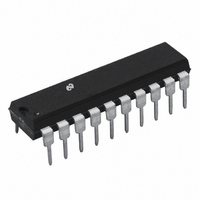
ADC0858CIN National Semiconductor, ADC0858CIN Datasheet - Page 13

ADC0858CIN
Manufacturer Part Number
ADC0858CIN
Description
IC DATA ACQUISITION/MON 20-DIP
Manufacturer
National Semiconductor
Type
Data Acquisition System (DAS)r
Datasheet
1.ADC0851BIN.pdf
(36 pages)
Specifications of ADC0858CIN
Resolution (bits)
8 b
Data Interface
NSC MICROWIRE™, Serial
Voltage Supply Source
Single Supply
Voltage - Supply
5V
Operating Temperature
-40°C ~ 85°C
Mounting Type
Through Hole
Package / Case
*
Lead Free Status / RoHS Status
Contains lead / RoHS non-compliant
Sampling Rate (per Second)
-
Other names
*ADC0858CIN
Available stocks
Company
Part Number
Manufacturer
Quantity
Price
Company:
Part Number:
ADC0858CIN
Manufacturer:
NSC
Quantity:
5 510
Company:
Part Number:
ADC0858CIN
Manufacturer:
HP
Quantity:
5 510
Pin Descriptions
V
OSC
CS
CLK
DI
DO
INT
EOC
CC
Positive power supply pin Bypass to analog
ground with a 0 1
parallel with a 10 F tantalum capacitor
Input Output pin used to generate internal
timing for A D conversion This pin is con-
nected to an external resistor and capacitor
to set the oscillation frequency for analog
timing (see Figure 12 )
This is the chip select input pin It must be
held low while data is transferred to or from
the ADC0851 8 (see Timing Diagram)
The serial clock input pin is used to clock
serial data either into the data input pin (DI)
or out of the data output pin (DO) Input data
is loaded on the rising edge of CLK and the
output data is valid at the falling edge of
CLK
Serial data digital input pin
TRI-STATE data output pin
This is the active low interrupt pin that indi-
cates that at least one analog input channel
voltage level has exceeded the pro-
grammed window limits Since this pin has
an open drain output an external pull up re-
sistor is required This allows many devices
to be wire-ORed together using a single
pull-up resistor
End of conversion output pin The low state
indicates that an A D conversion is in prog-
ress The EOC pin goes high when the con-
version is completed
F ceramic capacitor in
13
AGND
DGND
V
COM
CH0– CH1
(ADC0851)
CH0– CH7
(ADC0858)
COMPL
COMPH
REF
Analog ground reference
Digital ground reference for the logic inputs
Both AGND and DGND should be at same
potential
This is the analog reference pin The volt-
age applied to this pin sets the full scale
A D conversion range Recommended volt-
ages applied to this pin range from 1V to
V
ceramic capacitor in parallel with a 10 F
tantalum capacitor
The COM pin functions as an inverting dif-
ferential input common to all analog inputs
when each channel is configured as a sin-
gle-ended channel If the input channels are
programmed as differential pairs then the
COM input has no effect
CH0– CH7 are analog input channels which
can be configured as single ended inputs or
as differential pairs The analog input volt-
age should stay within the power supply
range
These output pins are available only on the
ADC0851 During ‘‘Watchdog’’ operation if
either of the inputs exceeds the window lim-
its not only is an interrupt generated but
also the COMPL and COMPH pins go low to
indicate whether the upper or lower bounda-
ry was exceeded (See applications section
for more information )
CC
Bypass to analog ground with a 0 1 F


