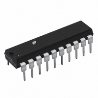
ADC0858CIN National Semiconductor, ADC0858CIN Datasheet - Page 25

ADC0858CIN
Manufacturer Part Number
ADC0858CIN
Description
IC DATA ACQUISITION/MON 20-DIP
Manufacturer
National Semiconductor
Type
Data Acquisition System (DAS)r
Datasheet
1.ADC0851BIN.pdf
(36 pages)
Specifications of ADC0858CIN
Resolution (bits)
8 b
Data Interface
NSC MICROWIRE™, Serial
Voltage Supply Source
Single Supply
Voltage - Supply
5V
Operating Temperature
-40°C ~ 85°C
Mounting Type
Through Hole
Package / Case
*
Lead Free Status / RoHS Status
Contains lead / RoHS non-compliant
Sampling Rate (per Second)
-
Other names
*ADC0858CIN
Available stocks
Company
Part Number
Manufacturer
Quantity
Price
Company:
Part Number:
ADC0858CIN
Manufacturer:
NSC
Quantity:
5 510
Company:
Part Number:
ADC0858CIN
Manufacturer:
HP
Quantity:
5 510
3 0 Watchdog Mode
4 0 A D Conversion Modes
The ADC0851 8 can be used in two A D conversion
modes In ‘‘One A D conversion’’ mode the device oper-
ates as a multiplexed A D converter and a conversion may
be initiated on any channel or channel pair configured in the
differential mode In the ‘‘Automatic A D conversion’’ mode
an A D conversion is done on a channel or channel pair and
after the output data is transmitted conversion begins on
the next subsequent channel or channel pair This process
will continue unless the device’s mode of operation is
changed
Note that the A D conversion time is determined by the
oscillator clock period and has no relation with the digital
clock signal CLK The oscillator clock’s frequency is set by
connecting a resistor from the OSC pin (pin 2 for ADC0851
or ADC0858) to V
ground The conversion time of the A D converter is eigh-
teen OSC clock periods maximum Assuming that the oscil-
lation clock frequency is set at 1 MHz (with R
and C
18 s maximum
4 1 ONE A D CONVERSION MODE
This mode is used to initiate one A D conversion on a single
channel or channel pair configured in the differential mode
The necessary mode address as per Table I is 1 0 1 0 The
format for the input word is as follows
Data Input (DI) word ADC0851 or ADC0858
(Table V(a) for ADC0851 Table V(b) for ADC0858)
ext
e
170 pF) then the conversion time would be
CC
and a capacitor from the OSC pin to
(Continued)
FIGURE 9 Status Bit Normalization
ext
TL H 11021 – 49
e
3 16 k
25
The 4-bit data following the mode address is the channel
information address These four bits assign the MUX config-
uration for the single A D conversion The channel informa-
tion addresses and the corresonding MUX configurations
are shown in Table V(a) and (b) for ADC0851 and ADC0858
respectively Note that the ADC0851 only decodes the two
LSBs of the channel information data while ignoring the two
MSBs (I3 and I2) When a channel pair is configured in the
differential mode it is important to note that the arithmetic
difference of the channel voltages should not be negative
Negative difference voltage would result in all zeroes at the
output
I3
X
X
X
X
Channel Information
TABLE V(a) Channel Information for
I2
X
X
X
X
One A D Conversion (ADC0851)
I1
0
0
1
1
I0
0
1
0
1
Channels Enabled
CH0
CH0 – CH1
CH1
Invalid
TL H 11021– 48


