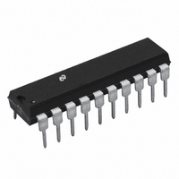
ADC0858CIN National Semiconductor, ADC0858CIN Datasheet - Page 20

ADC0858CIN
Manufacturer Part Number
ADC0858CIN
Description
IC DATA ACQUISITION/MON 20-DIP
Manufacturer
National Semiconductor
Type
Data Acquisition System (DAS)r
Datasheet
1.ADC0851BIN.pdf
(36 pages)
Specifications of ADC0858CIN
Resolution (bits)
8 b
Data Interface
NSC MICROWIRE™, Serial
Voltage Supply Source
Single Supply
Voltage - Supply
5V
Operating Temperature
-40°C ~ 85°C
Mounting Type
Through Hole
Package / Case
*
Lead Free Status / RoHS Status
Contains lead / RoHS non-compliant
Sampling Rate (per Second)
-
Other names
*ADC0858CIN
Available stocks
Company
Part Number
Manufacturer
Quantity
Price
Company:
Part Number:
ADC0858CIN
Manufacturer:
NSC
Quantity:
5 510
Company:
Part Number:
ADC0858CIN
Manufacturer:
HP
Quantity:
5 510
2 0 Memory Access Modes
The address bits access specific memory locations as per
Table II(a) and (b) for the ADC0851 and ADC0858 respec-
tively The address data is clocked in with the MSB (bit A3)
first
The timing diagram in Figure 5 shows that after CS goes
low the first four bits of the input word configure the device
to ‘‘read one limit’’ mode Next the address bits select the
desired memory location Third clock rising edge after the
address data’s LSB is loaded the limit data is output with
the LSB (bit L0) first
2 4 READ ALL LIMITS MODE
With a mode address of 1 1 1 1 the device is configured in
the ‘‘read all limits mode’’ When in this mode 8-bit limit
data from each memory location is serially transmitted out
The data format for the input word is as follows
Data Input (DI) Word ADC0851 or ADC0858
FIGURE 5 Timing Diagram for Read One Limit ADC0851 ADC0858
FIGURE 6 Timing Diagram for Read All Limits ADC0851 ADC0858
TL H 11021– 36
(Continued)
20
Note that no memory address data is required The limit
data is sequentially transmitted out starting from the memo-
ry location for CH0– Lower Limit and ending at CH1– Upper
Limit for the ADC0851 (see Table II(a)) CH7– Upper Limit
for the ADC0858 (see Table II(b))
The timing diagram of Figure 6 shows that the input data is
loaded starting at the first rising edge of CLK after CS goes
low Third clock rising edge after the last bit of the input data
is loaded the limit data is serially transmitted out Four limit
words are transmitted for the ADC0851 sixteen for the
ADC0858 Each limit word is output with the LSB (bit L0)
first Taking CS high after the MSB of the last limit data is
transmitted completes the operation
TL H 11021 – 39
TL H 11021 – 38


