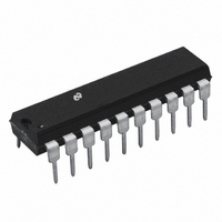
ADC0858CIN National Semiconductor, ADC0858CIN Datasheet - Page 26

ADC0858CIN
Manufacturer Part Number
ADC0858CIN
Description
IC DATA ACQUISITION/MON 20-DIP
Manufacturer
National Semiconductor
Type
Data Acquisition System (DAS)r
Datasheet
1.ADC0851BIN.pdf
(36 pages)
Specifications of ADC0858CIN
Resolution (bits)
8 b
Data Interface
NSC MICROWIRE™, Serial
Voltage Supply Source
Single Supply
Voltage - Supply
5V
Operating Temperature
-40°C ~ 85°C
Mounting Type
Through Hole
Package / Case
*
Lead Free Status / RoHS Status
Contains lead / RoHS non-compliant
Sampling Rate (per Second)
-
Other names
*ADC0858CIN
Available stocks
Company
Part Number
Manufacturer
Quantity
Price
Company:
Part Number:
ADC0858CIN
Manufacturer:
NSC
Quantity:
5 510
Company:
Part Number:
ADC0858CIN
Manufacturer:
HP
Quantity:
5 510
ure 10 After CS goes low the input word (DI) is clocked in
4 0 A D Conversion Modes
The timing diagram for one A D conversion is shown in Fig-
starting at the first rising edge of the digital clock signal
CLK The first four bits of the input word configure the de-
vice for ‘‘one A D conversion’’ mode while the following
four bits (channel information address) assign the configura-
tion of the MUX as per Table V(a) and (b) for the ADC0851
and the ADC0858 respectively Any input data following the
channel information address is ignored until the device’s
mode of operation is changed
Taking CS high after the last bit of the channel information
address loads the input word Had CS been kept low longer
the following bits of the input word would have been ig-
nored The device takes one to two OSC clock periods after
CS goes high to initiate the start of A D conversion The
EOC output goes low thus signalling the start of the conver-
sion process After a maximum of eighteen OSC clock peri-
ods conversion is completed and EOC output goes high
thus signalling the end of conversion The output data is
now available and will be transmitted only if CS is brought
low The output data is transmitted starting at the first rising
edge of CLK after CS goes low
I3
0
0
0
0
0
0
0
0
1
1
1
1
1
1
1
1
Channel Information
for One A D Conversion (ADC0858)
I2
0
0
0
0
1
1
1
1
0
0
0
0
1
1
1
1
TABLE V(b) Channel Information
I1
0
0
1
1
0
0
1
1
0
0
1
1
0
0
1
1
I0
0
1
0
1
0
1
0
1
0
1
0
1
0
1
0
1
Channels Enabled
CH0
CH0–CH1
CH1
Invalid
CH2
CH2–CH3
CH3
Invalid
CH4
CH4–CH5
CH5
Invalid
CH6
CH6–CH7
CH7
Invalid
(Continued)
26
The format for the output word is as shown below
The first eight bits of the output word represent the digital
equivalent of the input voltage Bits I3 through I0 provide the
channel configuration information as per Table V(a) and (b)
for ADC0851 and ADC0858 respectively Note that this in-
formation is the same as the channel information in the in-
put word The order in which the output data is transmitted
is as follows
Note that the output will be TRI-STATE if CS remains low
after I0 is transmitted Taking CS high after the output data
is transmitted causes the device to initiate the start of the
next A D conversion on the same input while ignoring the
data input word (DI) If the duration for which CS is high is
less than seventeen OSC clock periods the conversion pro-
cess will be interrupted and the device will look for the mode
address at the falling edge of CS so as to configure to a new
mode of operation However if CS is high for eighteen or
more OSC clock periods then the conversion operation will
continue from point A on the timing diagram (Figure 10)
To ensure repetitive A D conversion on the same input CS
going low should be synchronized with EOC going high
Thus after EOC goes high the conversion is completed and
CS can go low to transmit the output data Meanwhile if CS
goes low while EOC is low then the conversion process is
interrupted and the device is readied for a new mode of
operation
4 2 AUTO A D CONVERSION MODE
When used in this mode the ADC0851 8 offers added flexi-
bility that many multiplexed A D converters don’t In the
auto A D conversion mode the ADC0851 8 scans through
the selected input channels performing A D conversion on
each channel without the need for reloading a new data
input word each time From Table I the mode address for
the ‘‘Auto A D Conversion’’ mode is 1 1 1 0
The format for the input word is as follows
Data LSB (D0) first
Channel information MSB (I3) first
Data Input (DI) Word ADC0851 or ADC0858
Data Output (DO) ADC0851 or ADC0858
TL H 11021 – 50
TL H 11021 – 51


