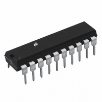
ADC0858CIN National Semiconductor, ADC0858CIN Datasheet - Page 23

ADC0858CIN
Manufacturer Part Number
ADC0858CIN
Description
IC DATA ACQUISITION/MON 20-DIP
Manufacturer
National Semiconductor
Type
Data Acquisition System (DAS)r
Datasheet
1.ADC0851BIN.pdf
(36 pages)
Specifications of ADC0858CIN
Resolution (bits)
8 b
Data Interface
NSC MICROWIRE™, Serial
Voltage Supply Source
Single Supply
Voltage - Supply
5V
Operating Temperature
-40°C ~ 85°C
Mounting Type
Through Hole
Package / Case
*
Lead Free Status / RoHS Status
Contains lead / RoHS non-compliant
Sampling Rate (per Second)
-
Other names
*ADC0858CIN
Available stocks
Company
Part Number
Manufacturer
Quantity
Price
Company:
Part Number:
ADC0858CIN
Manufacturer:
NSC
Quantity:
5 510
Company:
Part Number:
ADC0858CIN
Manufacturer:
HP
Quantity:
5 510
3 0 Watchdog Mode
The device will read the new input word and configure to a
different mode if CS is high for less than eight oscillator
clock periods for the ADC0851 and less than thirty-two os-
cillator clock periods for the ADC0858
Once a boundary limit is crossed INT goes low Moreover
for ADC0851 COMPL goes low if a lower limit is crossed
whereas COMPH goes low if an upper limit is crossed If the
input signals exceed both the upper and lower boundary
limits then both COMPL and COMPH would go low
To output data after a limit crossing occurs (i e after INT
goes low) CS should be brought low Note that INT
COMPL and COMPH would remain low as long as CS
doesn’t go low After CS goes low INT COMPL and
COMPH go high and one clock cycle later output data is
transmitted starting at the first rising edge of CLK however
the data is valid at the falling edge of CLK ( Figure 7 )
3 2 LIMIT CROSSING DETECTION
When the ADC0851 8 is configured in the watchdog mode
the device operates as a window comparator First the low-
er window limit (stored in the RAM) for CH0 is compared
against the input voltage at CH0 If the input voltage is
greater than the lower limit then no interrupt is generated
Next the upper window limit for CH0 is compared against
CH0 input voltage If the input voltage is less than the upper
window limit then no interrupt is generated for CH0 and the
device starts a similar comparison cycle for the next chan-
nel (CH1) Note that the lower limit can be greater than the
upper limit in this case the device will flag the microproces-
sor if the input signal falls inside a window
Tag
0
1
2
3
T3
0
0
0
0
TABLE IVa Channel Tag Address
Tag Address
T2
0
0
0
0
and Status (ADC0851)
T1
0
0
1
1
T0
0
1
0
1
(Continued)
Corresponding Limit
Lower Limit CH0
Upper Limit CH0
Lower Limit CH1
Upper Limit CH1
and Channel
TL H 11021 – 43
23
Each comparison takes 2 s thus a total of 4 s is required
per channel
When in watchdog mode the device will continuously cycle
through the input channels until an input that has crossed its
preset window limit is detected When this occurs a logical
‘‘1’’ is stored in the MSB (bit S3 for ADC0851 and S15 for
ADC0858) position of the status register In addition the tag
register is updated with the channel’s address (see Tables
IV(a) and (b) for ADC0851 and ADC0858 respectively) Note
that the tag address indicates which channel crossed which
limit Once the tag register is updated after the first limit is
crossed the device will once more cycle through the re-
maining channels and compare the input voltages against
Tag
10
11
12
13
14
15
0
1
2
3
4
5
6
7
8
9
T3
0
0
0
0
0
0
0
0
1
1
1
1
1
1
1
1
TABLE IVb Channel Tag Address
Tag Address
T2
0
0
0
0
1
1
1
1
0
0
0
0
1
1
1
1
and Status (ADC0858)
T1
0
0
1
1
0
0
1
1
0
0
1
1
0
0
1
1
T0
0
1
0
1
0
1
0
1
0
1
0
1
0
1
0
1
Corresponding Limit
Lower Limit CH0
Upper Limit CH0
Lower Limit CH1
Upper Limit CH1
Lower Limit CH2
Upper Limit CH2
Lower Limit CH3
Upper Limit CH3
Lower Limit CH4
Upper Limit CH4
Lower Limit CH5
Upper Limit CH5
Lower Limit CH6
Upper Limit CH6
Lower Limit CH7
Upper Limit CH7
and Channel
TL H 11021– 44


