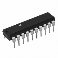
ADC0858CIN National Semiconductor, ADC0858CIN Datasheet - Page 21

ADC0858CIN
Manufacturer Part Number
ADC0858CIN
Description
IC DATA ACQUISITION/MON 20-DIP
Manufacturer
National Semiconductor
Type
Data Acquisition System (DAS)r
Datasheet
1.ADC0851BIN.pdf
(36 pages)
Specifications of ADC0858CIN
Resolution (bits)
8 b
Data Interface
NSC MICROWIRE™, Serial
Voltage Supply Source
Single Supply
Voltage - Supply
5V
Operating Temperature
-40°C ~ 85°C
Mounting Type
Through Hole
Package / Case
*
Lead Free Status / RoHS Status
Contains lead / RoHS non-compliant
Sampling Rate (per Second)
-
Other names
*ADC0858CIN
Available stocks
Company
Part Number
Manufacturer
Quantity
Price
Company:
Part Number:
ADC0858CIN
Manufacturer:
NSC
Quantity:
5 510
Company:
Part Number:
ADC0858CIN
Manufacturer:
HP
Quantity:
5 510
3 0 Watchdog Mode
This is the primary real time operating mode During watch-
dog operation the upper and lower limits stored in the RAM
are applied sequentially to the DAC’s digital inputs The
DAC’s analog output is applied to the comparator input and
compared against the voltage at the enabled analog input
pin The data format for the input word is as shown below
The last twelve bits of the input word assign the multiplexer
channel configuration
3 1 SELECTING THE CHANNEL CONFIGURATION
When the device is either in the watchdog or automatic A D
conversion mode each pair of analog input channels must
be programmed to determine which channel(s) will be ac-
tive and whether they will be operating single-ended or dif-
ferentially Table III(a) and (b) show the channel addresses
for the ADC0851 and the ADC0858 in various channel con-
figurations When the channels are configured as single-
ended inputs the input voltages are measured with respect
to the voltage at the COM pin Applying a DC voltage at the
Data Input (DI) Word ADC0851 or ADC0858
TABLE IIIa Multiplexer Channel Configuration (ADC0851)
TABLE IIIb Multiplexer Channel Configuration (ADC0858)
TL H 11021 – 37
21
COM pin will cause the device to measure the difference
between the input signal and the voltage at the COM pin
The voltage at the COM pin has no effect on an input chan-
nel that is configured as a differential pair When the chan-
nel pairs are configured as differential inputs (i e CH0 –
CH1 CH2 – CH3 etc ) the differential voltage is compared
with the limits for the lower numbered channel For exam-
ple the differential voltage CH0 – CH1 will be compared with
the limits for CH0 Note that the channel pairs are pro-
grammed in groups of three bits The channel address is
input to the A D converter with the MSB (bit C11) first
The timing diagrams for ADC0851 and ADC0858 watchdog
operation are shown in Figure 7 After a CS low is detected
the input word (DI) is clocked in starting at the first rising
edge of the serial clock (CLK) Once the least significant bit
of the channel address is loaded CS should go high Taking
CS high after the proper input word is loaded initiates the
operation of the device in the watchdog mode To keep the
device in continuous watchdog mode CS should remain
high for eight or more OSC clock periods for the ADC0851
and thirty-three or more OSC clock periods for the
ADC0858 If the input signals are within the boundary limits
the interrupt pin (INT) remains at logic ‘‘1’’ and the Data
Ouptut (DO) pin is in TRI-STATE In addition in the case of
the ADC0851 the COMPL and COMPH pins remain at logic
‘‘1’’
TL H 11021 – 40
TL H 11021 – 41


