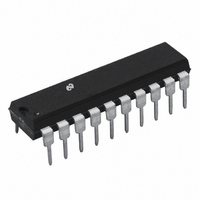
ADC0858CIN National Semiconductor, ADC0858CIN Datasheet - Page 30

ADC0858CIN
Manufacturer Part Number
ADC0858CIN
Description
IC DATA ACQUISITION/MON 20-DIP
Manufacturer
National Semiconductor
Type
Data Acquisition System (DAS)r
Datasheet
1.ADC0851BIN.pdf
(36 pages)
Specifications of ADC0858CIN
Resolution (bits)
8 b
Data Interface
NSC MICROWIRE™, Serial
Voltage Supply Source
Single Supply
Voltage - Supply
5V
Operating Temperature
-40°C ~ 85°C
Mounting Type
Through Hole
Package / Case
*
Lead Free Status / RoHS Status
Contains lead / RoHS non-compliant
Sampling Rate (per Second)
-
Other names
*ADC0858CIN
Available stocks
Company
Part Number
Manufacturer
Quantity
Price
Company:
Part Number:
ADC0858CIN
Manufacturer:
NSC
Quantity:
5 510
Company:
Part Number:
ADC0858CIN
Manufacturer:
HP
Quantity:
5 510
Figure 13 shows the overvoltage protection circuit for the
3 0 The Analog Inputs
resistance Another source of error is the sampling nature of
the A D converter Short spikes of current enter the ‘‘
input and exit the ‘‘
sition of the OSC clock These currents decay rapidly and
generally do not cause errors since the internal comparator
is strobed at the end of a clock period If large source resist-
ances are used however then the transients caused by the
current spikes may not settle completely before conversion
begins If a capacitor is used at the input of the A D convert-
er for input filtering then the input signal source resistance
should be kept at 1 k
3 3 ANALOG INPUT PROTECTION
Often the analog inputs of A D converters are driven from
voltage sources that can swing higher than V
than GND Analog inputs often come from op amps which
use
voltages stay within the 0V–5V A D converter supply volt-
age range at power up the input voltage may actually rise
above or fall below the A D converter’s supply voltages If
the input voltage to any A D converter input pin does fall
outside the supply voltage by more than 0 3V (worst case)
and the input draws more than 5 mA then there is a good
possibility that the converter may latch up and provide a low
impedance short between V
analog input If for instance the amplifier’s output saturates
to its positive supply rail then the junction of R1 and R2
would be clamped to V
limits the op amp’s output current and R2 limits the current
flowing into the input of the A D converter Likewise the
junction of R1 and R2 would be clamped to a diode drop
below ground if the op amp’s output saturates to the nega-
tive rail
4 0 Zero Scale and Full Scale
Adjustment
4 1 ZERO SCALE ERROR
The zero scale error of the A D converter does not require
adjustment If the minimum analog input voltage value
V
done The converter can be made to output 0000 0000 digi-
tal code for this minimum input voltage by biasing the V
Typical Applications
IN(Min)
g
15V supplies While during normal operation the input
is not at ground potential then a zero offset can be
b
’’ input at the rising and falling tran-
or less
CC
plus a diode drop Resistor R1
FIGURE 12 Recommended Connection for ADC0851 and ADC0858
CC
and GND
(Continued)
CC
or lower
IN(
a
b
’’
)
30
input of a differential input pair at this V
utilizes the differential mode operation of the A D converter
The zero scale error of the A D converter relates to the
location of the first riser of the transfer function and can be
measured by grounding the V
small magnitude positive voltage to the V
error is the difference between the actual DC input voltage
(the ideal
V
digital code transition from 0000 0000 to 0000 0001
4 2 FULL SCALE ADJUSTMENT
The full-scale adjustment can be made by applying an input
voltage that is 1 5 LSB less than the desired analog full-
scale voltage and then adjusting the magnitude of the V
input voltage for a digital output code that just changes from
1111 1110 to 1111 1111
4 3 ADJUSTING FOR AN ARBITRARY
ANALOG INPUT VOLTAGE RANGE
Analog input voltages that span from a positive non-zero
minimum value can easily be accommodated by the
ADC0851 8 In this case the A D converter is used in the
differential mode and a reference voltage equal to V
is applied to the V
ment is not required because the zero scale error is very
small However if zero scale adjustment is desired then a
voltage equal to V
voltage span 256) should be applied to V
erence voltage at V
output code just changes from 0000 0000 to 0000 0001
Once the proper reference voltage is applied to the V
input then full scale adjustment can be made Full scale
adjustment is made by first applying a voltage to the V
input that is 1 5 LSB less than V
where V
The reference voltage V
pin of the A D converter is adjusted so that the output code
just changes from 1111 1110 to 1111 1111 This completes
the adjustment procedure
DC
) and the applied input voltage that causes an output
V
IN(
V
Max
Min
a
) FS ADJ
LSB value
e
e
the high end of the analog input voltage
range
the low end of the analog input voltage
range
IN(Min)
e
IN(
IN(
b
V
b
Max
)
)
plus
input Normally zero scale adjust-
REF
should be adjusted such that the
LSB
b
applied to the reference input
1 5 (V
IN(
e
LSB (where 1 LSB
IN(Max)
b
9 8 mV for V
)
Max
input and applying a
i e
b
IN(Min)
IN(
IN(
V
a
a
Min
)
REF
)
TL H 11021 – 55
and the ref-
) 256
value This
input Zero
e
e
IN(Min)
5 000
IN(
Input
IN(
REF
b
a
)
)


