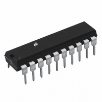
ADC0858CIN National Semiconductor, ADC0858CIN Datasheet - Page 5

ADC0858CIN
Manufacturer Part Number
ADC0858CIN
Description
IC DATA ACQUISITION/MON 20-DIP
Manufacturer
National Semiconductor
Type
Data Acquisition System (DAS)r
Datasheet
1.ADC0851BIN.pdf
(36 pages)
Specifications of ADC0858CIN
Resolution (bits)
8 b
Data Interface
NSC MICROWIRE™, Serial
Voltage Supply Source
Single Supply
Voltage - Supply
5V
Operating Temperature
-40°C ~ 85°C
Mounting Type
Through Hole
Package / Case
*
Lead Free Status / RoHS Status
Contains lead / RoHS non-compliant
Sampling Rate (per Second)
-
Other names
*ADC0858CIN
Available stocks
Company
Part Number
Manufacturer
Quantity
Price
Company:
Part Number:
ADC0858CIN
Manufacturer:
NSC
Quantity:
5 510
Company:
Part Number:
ADC0858CIN
Manufacturer:
HP
Quantity:
5 510
AC Electrical Characteristics
The following specifications apply for V
5 ns unless otherwise specified Boldface limits apply for T
Note 1 Absolute Maximum Ratings indicate limits beyond which damage to the device may occur Operating Ratings indicate conditions for which the device is
functional but do not guarantee specific performance limits For guaranteed specifications and test conditions see the Electrical Characteristics The guaranteed
specifications apply only for the test conditions listed Some performance characteristics may degrade when the device is not operated under the listed test
conditions
Note 2 All voltages are measured with respect to ground (AGND
Note 3 All of the analog and digital input pins are internally diode clamped to the supply pins Should the applied voltage at any pin exceed the power supply
voltage the additional absolute value of current at that pin (caused by the forward biasing of the internal diodes) should be limited to 5 mA or less
Note 4 Human body model 100 pF discharged through a 1 5 k
Note 5 Typical specifications are at
Note 6 Tested limits are guaranteed to National’s AOQL (Average Outgoing Quality Level)
Note 7 Total unadjusted error includes comparator offset ADC linearity and multiplexer error and is expressed in LSBs
Note 8 Two on-chip diodes are tied to each analog input The diodes will forward conduct for analog input voltages one diode drop below ground or one diode drop
above V
diodes to conduct especially at elevated temperatures This will cause errors for analog inputs near full scale The specification allows 50 mV forward bias of either
clamp diode Thus as long as V
to 5 V
Note 9 Leakage current is measured with the oscillator clock disabled
Note 10 Measured supply current does not include the DAC ladder current
Note 11 A 40% to 60% clock duty cycle range ensures proper operation at all clock frequencies
Symbol
t
f
t
t
t
C
C
1H
OSC
EOC
Conv
CS-INT
IN
OUT
DC
t
0H
CC
input voltage range will therefore require a minimum supply voltage of 4 950 V
Care should be exercised when operating the device at low supply voltages (e g V
Rising Edge of CS to
Data Output Hi-Z
Oscillator Clock Freq
(Analog Timing)
CS to End of
Conversion Delay
Conversion Time
CS to Interrupt Delay
Capacitance of
Logic Input
Capacitance of
Logic Output
Parameter
IN
or V
a
REF
25 C and represent the most likely parametric norm
does not exceed the supply voltage by more than 50 mV the output code will be correct To achieve an absolute 0 V
CC
e a
5 V
(Continued)
C
(See TRI-STATE
Test Circuits)
R
C
ext
ext
e
DC
e
resistor
Conditions
e
100 pF R
e
DGND
V
3 16 k
170 pF
REF
A
e
e a
e
5
0V)
e
T
J
4 5 V
2k
e
DC
T
DC
MIN
CC
AGND
to T
e
(Note 5)
Typical
4 5V) because high analog inputs (5V) can cause the input
MAX
90
60
1
5
5
e
all other limits apply at T
DGND
e
(Note 6)
0V f
Limit
200
120
1 4
0 6
17
18
1
2
CLK
e
1 MHz t
A
e
OSC Clock
OSC Clock
MHz (Max)
MHz (Min)
T
ns (Max)
ns (Max)
(Limits)
Periods
Periods
J
(Max)
Units
(Min)
Max
r
Min
e
pF
pF
e
25 C
t
f
e
DC


