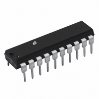
ADC0858CIN National Semiconductor, ADC0858CIN Datasheet - Page 18

ADC0858CIN
Manufacturer Part Number
ADC0858CIN
Description
IC DATA ACQUISITION/MON 20-DIP
Manufacturer
National Semiconductor
Type
Data Acquisition System (DAS)r
Datasheet
1.ADC0851BIN.pdf
(36 pages)
Specifications of ADC0858CIN
Resolution (bits)
8 b
Data Interface
NSC MICROWIRE™, Serial
Voltage Supply Source
Single Supply
Voltage - Supply
5V
Operating Temperature
-40°C ~ 85°C
Mounting Type
Through Hole
Package / Case
*
Lead Free Status / RoHS Status
Contains lead / RoHS non-compliant
Sampling Rate (per Second)
-
Other names
*ADC0858CIN
Available stocks
Company
Part Number
Manufacturer
Quantity
Price
Company:
Part Number:
ADC0858CIN
Manufacturer:
NSC
Quantity:
5 510
Company:
Part Number:
ADC0858CIN
Manufacturer:
HP
Quantity:
5 510
2 0 Memory Access Modes
The ADC0851 8 has an internal RAM with sixteen memory
locations (one location for the upper limit and one for the
lower limit for each of the 8 input channels) Each memory
location is 8 bits wide An 8-bit limit word representing an
upper or lower limit boundary can either be written to or read
from the RAM The ADC0851 uses only four memory loca-
tions for the four boundary limits corresponding to the two
inputs The eight channel ADC0858 however makes use of
all sixteen memory locations
Each memory location is accessed by a specific address as
shown by Table II(a) and (b) Note that even addresses cor-
respond to the lower limits while the odd addresses corre-
spond to the upper limits The ADC0851 and ADC0858 both
use 4 bits (A3
ADC0851 decodes only the two LSBs of the address data
while ignoring the two MSBs
L0
L0
A3
A3
X
X
X
X
0
0
0
0
0
0
0
0
1
1
1
1
1
1
1
1
L1
L1
RAM Address
RAM Address
A2
A2
X
X
X
X
0
0
0
0
1
1
1
1
0
0
0
0
1
1
1
1
L2
L2
TABLE IIa RAM Address and
TABLE IIb RAM Address and
Limit Data for ADC0851
Limit Data for ADC0858
Limit Data (ADC0851)
Limit Data (ADC0858)
L3
L3
A1
A1
0
0
1
1
0
0
1
1
0
0
1
1
0
0
1
1
0
0
1
1
A0) to address the RAM however
L4
L4
A0
A0
0
1
0
1
0
1
0
1
0
1
0
1
0
1
0
1
0
1
0
1
L5
L5
CH0–Lower Limit
CH0–Upper Limit
CH1–Lower Limit
CH1–Upper Limit
CH0–Lower Limit
CH0–Upper Limit
CH1–Lower Limit
CH1–Upper Limit
CH2–Lower Limit
CH2–Upper Limit
CH3–Lower Limit
CH3–Upper Limit
CH4–Lower Limit
CH4–Upper Limit
CH5–Lower Limit
CH5–Upper Limit
CH6–Lower Limit
CH6–Upper Limit
CH7–Lower Limit
CH7–Upper Limit
Channel and Limit
Channel and Limit
L6
L6
Corresponding
Corresponding
L7
L7
18
2 1 WRITE ONE LIMIT
This mode is used to update a single memory location in the
limit RAM An 8-bit limit word is written to the location point-
ed to by the limit address From Table I we can see that to
initiate the operation of the device in the ‘‘write one limit’’
mode the mode address has to be 1 0 0 1 The data format
for the input word is as shown below
Data Input (DI) Word ADC0851 or ADC0858
TL H 11021 – 31


