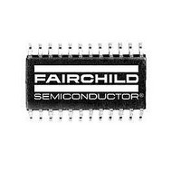
FAN5071M Fairchild Semiconductor, FAN5071M Datasheet - Page 11

FAN5071M
Manufacturer Part Number
FAN5071M
Description
DC/DC Switching Controllers DC/DC
Manufacturer
Fairchild Semiconductor
Datasheet
1.FAN5069MTCX.pdf
(22 pages)
Specifications of FAN5071M
Number Of Outputs
2
Output Voltage
1.05 V to 1.825 V
Output Current
28 A
Input Voltage
4.5 V to 5.25 V
Mounting Style
SMD/SMT
Package / Case
SOIC-24 Wide
Maximum Operating Temperature
+ 70 C
Minimum Operating Temperature
0 C
Lead Free Status / Rohs Status
Lead free / RoHS Compliant
Available stocks
Company
Part Number
Manufacturer
Quantity
Price
Part Number:
FAN5071M
Manufacturer:
FIR
Quantity:
20 000
Part Number:
FAN5071MX
Manufacturer:
FAIRCHILD/仙童
Quantity:
20 000
FAN5069 Rev. 1.1.5
© 2005 Fairchild Semiconductor Corporation
PWM Operation
Refer to Figure 20 for the PWM control mechanism. The
FAN5069 uses the summing mode method of control to
generate the PWM pulses. The amplified output of the
current-sense amplifier is summed with an internally
generated ramp and the combined signal is amplified
and compared with the output of the error amplifier to get
the pulse width to drive the high-side MOSFET. The
sensed current from the previous cycle is used to modu-
late the output of the summing block. The output of the
summing block is also compared against the voltage
threshold set by the R
rent on a cycle-by-cycle basis. The controller facilitates
external compensation for enhanced flexibility.
Initialization
When the PWM is disabled, the SW node is connected
to GND through an internal 500Ω MOSFET to slowly dis-
charge the output. As long as the PWM controller is
enabled, this internal MOSFET remains OFF.
Soft-Start (PWM and LDO)
When V
the circuit releases SS and enables the PWM regulator.
The capacitor connected to the SS pin and GND is
charged by a 10µA internal current source, causing the
voltage on the capacitor to rise. When this voltage
exceeds 1.2V, all protection circuits are enabled. When
this voltage exceeds 2.2V, the LDO output is enabled.
The input to the error amplifier at the non-inverting pin is
clamped by the voltage on the SS pin until it crosses the
reference voltage.
The time it takes the PWM output to reach regulation
(T
Oscillator Clock Frequency (PWM)
The clock frequency on the oscillator is set using an
external resistor, connected between R(T) pin and
ground. The frequency follows the graph, as shown in
Figure 18. The minimum clock frequency is 200KHz,
which is when R(T) pin is left open. Select the value of
R(T) as shown in the equation below. This equation is
valid for all F
where F
For example, for F
R
The FAN5069 provides for input voltage feed-forward
compensation through R
tively changes the slope of the internal ramp, minimizing
the variation of the PWM modulator gain when input volt-
T
R T ( )
RISE
RAMP
Rise
) is calculated using the following equation:
=
=
CC
OSC
Selection and Feed-Forward Operation
-------------------------------------------------- - Ω
(
8 10
F
OSC
exceeds the UVLO threshold and EN is high,
×
is in Hz.
OSC
5
–
–
×
2
> 200kHz.
200
×
OSC
10
C
9
LIM
×
SS
= 300kHz, R(T) = 50KΩ.
10
RAMP
resistor to limit the inductor cur-
(C
3
)
SS
. The value of R
is in μf)
RAMP
(EQ. 2)
(EQ. 3)
effec-
11
age varies. The R
limit, as can be seen in the R
R
equation:
where F
and V
Gate Drive Section
The adaptive gate control logic translates the internal
PWM control signal into the MOSFET gate drive signals
and provides necessary amplification, level shifting, and
shoot-through protection. It also has functions that help
optimize the IC performance over a wide range of oper-
ating conditions. Since the MOSFET switching time can
vary dramatically from device to device and with the
input voltage, the gate control logic provides adaptive
dead time by monitoring the gate-to-source voltages of
both upper and lower MOSFETs. The lower MOSFET
drive is not turned on until the gate-to-source voltage of
the upper MOSFET has decreased to less than approxi-
mately 1V. Similarly, the upper MOSFET is not turned on
until the gate-to-source voltage of the lower MOSFET
has decreased to less than approximately 1V. This
allows a wide variety of upper and lower MOSFETs to be
used without a concern for simultaneous conduction, or
shoot-through.
A low impedance path between the driver pin and the
MOSFET gate is recommended for the adaptive dead-
time circuit to work properly. Any delay along this path
reduces the delay generated by the adaptive dead-time
circuit, thereby increasing the chances for shoot-through.
Protection
In the FAN5069, the converter is protected against
extreme overload, short-circuit, over-voltage, and under-
voltage conditions. All of these conditions generate an
internal “fault latch” which shuts down the converter. For
all fault conditions both the high-side and the low-side
drives are off except in the case of OVP where the low-
side MOSFET is turned on until the voltage on the FB pin
goes below 0.4V. The fault latch can be reset either by
toggling the EN pin or recycling V
Over Current Limit (PWM)
The PWM converter is protected against overloading
through a cycle-by-cycle current limit set by selecting
R
threshold voltage for the output of the summing amplifier.
When the summing amplifier output exceeds this thresh-
old level, the current limit comparator trips and the PWM
starts skipping pulses. If the current limit tripping occurs
for 16 continuous clock cycles, a fault latch is set and the
controller shuts down the converter. This shutdown fea-
R
RAMP
ILIM
RAMP
IN
resistor. An internal 10µA current source sets the
value can be approximated using the following
= 12V, R
OSC
=
---------------------------------------------
6.3 10
is in Hz. For example, for F
•
V
IN
RAMP
RAMP
–
–
8
1.8
•
Fosc
≈
also has an effect on the current
540KΩ.
KΩ
LIM
CC
equation (EQ. 5). The
to the chip.
OSC
www.fairchildsemi.com
= 300kHz
(EQ. 4)


