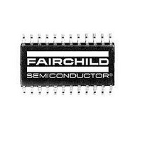
FAN5071M Fairchild Semiconductor, FAN5071M Datasheet - Page 13

FAN5071M
Manufacturer Part Number
FAN5071M
Description
DC/DC Switching Controllers DC/DC
Manufacturer
Fairchild Semiconductor
Datasheet
1.FAN5069MTCX.pdf
(22 pages)
Specifications of FAN5071M
Number Of Outputs
2
Output Voltage
1.05 V to 1.825 V
Output Current
28 A
Input Voltage
4.5 V to 5.25 V
Mounting Style
SMD/SMT
Package / Case
SOIC-24 Wide
Maximum Operating Temperature
+ 70 C
Minimum Operating Temperature
0 C
Lead Free Status / Rohs Status
Lead free / RoHS Compliant
Available stocks
Company
Part Number
Manufacturer
Quantity
Price
Part Number:
FAN5071M
Manufacturer:
FIR
Quantity:
20 000
Part Number:
FAN5071MX
Manufacturer:
FAIRCHILD/仙童
Quantity:
20 000
FAN5069 Rev. 1.1.5
© 2005 Fairchild Semiconductor Corporation
LDO Section
The LDO controller is designed to provide ultra low volt-
ages, as low as 0.8V for GTL-type loads. The regulating
loop employs a very fast response feedback loop and
small capacitors can be used to keep track of the chang-
ing output voltage during transients. For stable opera-
tion, the minimum capacitance on the output needs to be
100µF and the typical ESR needs to be around 100mΩ.
The maximum voltage at the gate drive for the MOSFET
can reach close to 0.5V below the V
For example, for a 1.2V output, the minimum enhance-
ment voltage required with 4.75V on V
(4.75V-0.5V-1.2V = 3.05V). The drop-out voltage for the
LDO is dependent on the load current and the MOSFET
chosen. It is recommended to use low enhancement
voltage MOSFETs for the LDO. In applications where
LDO is not needed, pull up the FBLDO pin (Pin #1)
higher than 1V to disable the LDO.
The soft-start on the LDO output (ramp) is controlled by
the capacitor on the SS pin to GND. The LDO output is
enabled only when the voltage on the SS pin reaches
2.2V. Refer to Figure 9 for start-up waveform.
Design Section
General Design Guidelines
Establishing the input voltage range and maximum cur-
rent loading on the converter before choosing the switch-
ing frequency and the inductor ripple current is highly
recommended. There are design trade-offs in choosing
an optimum switching frequency and the ripple current.
The input voltage range should accommodate the worst-
case input voltage with which the converter may ever
operate. This voltage needs to account for the cable drop
encountered from the source to the converter. Typically,
the converter efficiency tends to be higher at lower input
voltage conditions.
When selecting maximum loading conditions, consider
the transient and steady-state (continuous) loading sep-
arately. The transient loading affects the selection of the
inductor and the output capacitors. Steady state loading
affects the selection of MOSFETs, input capacitors, and
other critical heat-generating components.
The selection of switching frequency is challenging.
While higher switching frequency results in smaller com-
ponents, it also results in lower efficiency. Ideal selection
of switching frequency takes into account the maximum
operating voltage. The MOSFET switching losses are
directly proportional to F
the input voltage.
When selecting the inductor, consider the minimum and
maximum load conditions. Lower inductor values pro-
duce better transient response, but result in higher ripple
and lower efficiency due to high RMS currents. Optimum
minimum inductance value enables the converter to
SW
and the square function of
CC
of the controller.
CC
is 3.05V
13
operate at the boundary of continuous and discontinuous
conduction modes.
Setting the Output Voltage (PWM)
The internal reference for the PWM controller is at 0.8V.
The output voltage of the PWM regulator can be set in
the range of 0.8V to 90% of its power input by an exter-
nal resistor divider. The output is divided down by an
external voltage divider to the FB pin (for example, R1
and R
by the following equation:
To minimize noise pickup on this node, keep the resistor
to GND (R
Inductor Selection (PWM)
When the ripple current, switching frequency of the con-
verter, and the input-output voltages are established,
select the inductor using the following equation:
where I
This number typically varies between 20% to 50% of the
maximum steady-state load on the converter.
When selecting an inductor from the vendors, select the
inductance value which is close to the value calculated at
the rated current (including half the ripple current).
Input Capacitor Selection (PWM)
The input capacitors must have an adequate RMS cur-
rent rating to withstand the temperature rise caused by
the internal power dissipation. The combined RMS cur-
rent rating for the input capacitor should be greater than
the value calculated using the following equation:
Common capacitor types used for such application
include aluminum, ceramic, POS CAP, and OSCON.
Output Capacitor Selection (PWM)
The output capacitors chosen must have low enough
ESR to meet the output ripple and load transient require-
ments. The ESR of the output capacitor should be lower
than both of the values calculated below to satisfy both
the transient loading and steady-state ripple conditions
as given by the following equation:
V
L
I
ESR
INPUT RMS
MIN
OUT
≤
=
BIAS
(
=
Ripple
--------------------------------- -
ΔI
⎛
⎝
------------------------------------------- -
0.8V
V
LOAD MAX
I
BIAS
V
as in Figure 24). The output voltage is given
Ripple
OUT
)
STEP
is the ripple current.
=
) below 10KΩ.
×
(
I
–
LOAD MAX
⎛
⎝
×
1
V
--------------
V
OUT
F
+
)
IN
SW
--------------- -
R
(
and
R1
BIAS
2
⎞
⎠
)
⎞
⎠
×
ESR
⎛
⎜
⎝
V
--------------
V
OUT
≤
IN
V
------------------ -
I
Ripple
Ripple
–
⎛
⎝
V
--------------
V
OUT
IN
www.fairchildsemi.com
⎞
⎠
2
⎞
⎟
⎠
(EQ. 6)
(EQ. 7)
(EQ. 8)
(EQ. 9)


