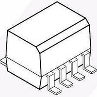
FL7930BM Fairchild Semiconductor, FL7930BM Datasheet - Page 12

FL7930BM
Manufacturer Part Number
FL7930BM
Description
Power Factor Correction ICs PFC Controller for Lighting; 2nd OVP
Manufacturer
Fairchild Semiconductor
Datasheet
1.FL7930BM.pdf
(20 pages)
Specifications of FL7930BM
Switching Frequency
300 KHz
Maximum Operating Temperature
+ 125 C
Mounting Style
SMD/SMT
Package / Case
SOP-8
Minimum Operating Temperature
- 40 C
Lead Free Status / Rohs Status
Lead free / RoHS Compliant
© 2011 Fairchild Semiconductor Corporation
FL7930 • Rev. 1.0.0
Applications Information
1. Startup: Normally, supply voltage (V
block is fed from the additional power supply, which can
be called standby power. Without this standby power,
auxiliary winding for zero current detection can be used
as a supply source. Once the supply voltage of the PFC
block exceeds 12V, internal operation is enabled until
the voltage drops to 8.5V. If V
current is sinking from V
2. INV Block: Scaled-down voltage from the output is
the input for the INV pin. Many functions are embedded
based on the INV pin: transconductance amplifier,
output OVP comparator, and disable comparator.
For the output voltage control, a transconductance
amplifier is used instead of the conventional voltage
amplifier. The transconductance amplifier (voltage-
controlled current source) aids the implementation of
OVP and disable functions. The output current of the
amplifier changes according to the voltage difference of
the inverting and non-inverting input of the amplifier. To
cancel down the line input voltage effect on power factor
correction, effective control response of PFC block
should be slower than the line frequency. This conflicts
with the transient response of controller. Two-pole one-
zero type compensation may be used to meet both
requirements.
The OVP comparator shuts down the output drive block
when the voltage of the INV pin is higher than 2.675V
with
disables operation when the voltage of the inverting
input is lower than 0.35V with 100mV hysteresis. An
external small-signal MOSFET can be used to disable
the IC. The IC operating current decreases to reduce
power consumption if the IC is disabled. Figure 27 is the
timing chart of the internal circuit near the INV pin when
rated-PFC output voltage is assumed at 390V
V
CC
supply voltage is 15V.
0.175V
Figure 25. Startup Circuit
hysteresis.
CC
.
The
CC
disable
exceeds V
CC
) of a PFC
comparator
Z
, 20mA
DC
and
12
3.
embedded by the information at the INV pin. That
information comes from the output through the voltage
dividing resistors. To scale down from high voltage to
low voltage, high resistance normally replaced with low
resistance. If the resistor of high resistance is damaged
and resistance is changed to high, INV pin information is
normal, but output voltage exceeds its rated output.
Once this occurs, output electrolytic capacitor may be
damaged. The FL3930B provides an additional OVP pin
that can be used to shut down the boost power stage
when output voltage exceeds the OVP level if the
resistors connected at the INV pin are damaged. To
prevent such a catastrophe, an additional OVP pin is
assigned to double check output voltage. The additional
OVP may be called second OVP, while INV pin OVP
can be called the first OVP. Since the two OVP
conditions are quite different, the protection recovery
modes are different.
OVP
Figure 27. Timing Chart for INV Block
Figure 26. Circuit Around INV Pin
Pin: Over-Voltage Protection
www.fairchildsemi.com
(OVP) is


