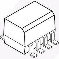
FL7930BM Fairchild Semiconductor, FL7930BM Datasheet - Page 18

FL7930BM
Manufacturer Part Number
FL7930BM
Description
Power Factor Correction ICs PFC Controller for Lighting; 2nd OVP
Manufacturer
Fairchild Semiconductor
Datasheet
1.FL7930BM.pdf
(20 pages)
Specifications of FL7930BM
Switching Frequency
300 KHz
Maximum Operating Temperature
+ 125 C
Mounting Style
SMD/SMT
Package / Case
SOP-8
Minimum Operating Temperature
- 40 C
Lead Free Status / Rohs Status
Lead free / RoHS Compliant
© 2011 Fairchild Semiconductor Corporation
FL7930 • Rev. 1.0.0
12. Current Sense: The MOSFET current is sensed
using an external sensing resistor for the over-current
protection. If the CS pin voltage is higher than 0.8V, the
over-current
protection signal. An internal RC filter of 40kΩ and 8pF
is included to filter switching noise.
13. Gate Driver Output: FL7930 contains a single
totem-pole output stage designed for a direct drive of
the power MOSFET. The drive output is capable of up
to +500/-800mA peak current with a typical rise and fall
time of 50ns with 1nF load. The output voltage is
clamped to 13V to protect the MOSFET gate even if the
V
14. PCB Layout
PFC block normally handles high switching current and
the voltage low-energy signal path can be affected by
the high-energy path. Cautious PCB layout is mandatory
for stable operation.
CC
voltage is higher than 13V.
The gate drive path should be as short as possible.
The closed-loop that starts from the gate driver,
MOSFET gate, and MOSFET source to ground of
PFC controller is recommended as close as
possible. This is also the crossing point between
power ground and signal ground. Power ground
path from the bridge diode to the output bulk
capacitor should be short and wide. The sharing
position between power ground and signal ground
should be only at one position to avoid ground loop
noise. Signal path of PFC controller should be short
and wide for external components to contact.
PFC output voltage sensing resistor is normally
high to reduce current consumption. This path can
be affected by external noise. To reduce noise
possibility at the INV pin, a shorter path for output
sensing is recommended. If a shorter path is not
possible, place some dividing resistors between
PFC output and the INV pin — closer to the INV pin
is better. Relative high voltage close to the INV pin
can be helpful.
protection
comparator
generates
a
18
ZCD path is recommended close to auxiliary
winding from boost inductor and to the ZCD pin. If
that is difficult, place a small capacitor (below 50pF)
to reduce noise.
Switching current-sense path should not share with
any other path to avoid interference. Some
additional components may be needed to reduce
the noise level applied to the CS pin.
A stabilizing capacitor for V
close as possible to the V
difficult, place the SMD capacitor as close to the
corresponding pins as possible.
Figure 48. Recommended PCB Layout
CC
CC
and ground pins. If it is
is recommended as
www.fairchildsemi.com


