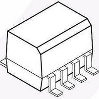
FL7930BM Fairchild Semiconductor, FL7930BM Datasheet - Page 13

FL7930BM
Manufacturer Part Number
FL7930BM
Description
Power Factor Correction ICs PFC Controller for Lighting; 2nd OVP
Manufacturer
Fairchild Semiconductor
Datasheet
1.FL7930BM.pdf
(20 pages)
Specifications of FL7930BM
Switching Frequency
300 KHz
Maximum Operating Temperature
+ 125 C
Mounting Style
SMD/SMT
Package / Case
SOP-8
Minimum Operating Temperature
- 40 C
Lead Free Status / Rohs Status
Lead free / RoHS Compliant
© 2011 Fairchild Semiconductor Corporation
FL7930 • Rev. 1.0.0
Once the first OVP triggers, switching stops immediately
and recovers switching when the output voltage is
decreased with a hysteresis. When the second OVP
triggers, switching can be recovered only when the V
supply voltage falls below V
than V
the second OVP is not used, the OVP pin must be
connected to the INV pin or to ground.
4. RDY Output: The FL7930C provides a PFC-ready
pin that can be used to trigger other power stages when
PFC output voltage reaches the proper level with
hysteresis. When the INV voltage is higher than 2.24V,
RDY out is triggered HIGH and lasts until the INV
voltage is lower than 2.051V. When input AC voltage is
quite high, for example 240V
always higher than RDY threshold, regardless of boost
converter operation. In this case, the INV voltage is
already higher than 2.24V before PFC V
V
not pulled LOW because the INV voltage is higher than
the RDY threshold. When V
5V, RDY is pulled LOW even through PFC output
voltage is higher than threshold. The RDY pin output is
open-drain, so needs an external pull-up resistor to
supply the proper power source. The RDY pin output
remains floating until V
START
Figure 28. Comparison of First and Second OVP
Figure 29. Two Cases of RDY Triggered HIGH
. After boost converter operation stops, RDY is
START
again and V
Recovery Modes
CC
OVP
is higher than 2V.
CC
is lower than hysteresis. If
STOP
AC
of the PFC drops below
, PFC output voltage is
and builds up higher
CC
touches
CC
13
5. Control Range Compensation: On time is controlled
by the output voltage compensator. When input voltage
is high and load is light, the control range becomes
narrow compared to when input voltage is low. That
control range decrease is anti-proportional to the double
square of the input voltage. Thus, at high line, unwanted
burst operation can occur at light load and audible noise
may be generated from the boost inductor or inductor at
input filter. Unlike other converters, burst operation in
PFC block is not needed because the PFC block itself is
normally disabled in Standby Mode. To reduce
unwanted burst operation at light load, internal control
range compensation is implemented and no burst
operation occurs until 5% load at high line.
6. Zero-Current Detection: Zero-Current Detection
(ZCD) generates the turn-on signal of the MOSFET
when the boost inductor current reaches zero using an
auxiliary winding coupled with the inductor. When the
power switch turns on, negative voltage is induced at the
auxiliary winding due to the opposite winding direction
(see Equation 1) and positive voltage is induced (see
Equation 2) when the power switch turns off.
V
where V
T
turns, respectively; V
converter; and V
PFC converter.
V
AUX
AUX
AUX
Figure 30. Two Cases of RDY Triggered LOW
are boost inductor turns and auxiliary winding
T
T
AUX
T
AUX
IND
T
AUX
IND
Figure 31. Circuit Near ZCD
is the auxiliary winding voltage; T
V
V
PFCOUT
AC
OUT_PFC
AC
V
is output voltage from the
AC
is input voltage for PFC
www.fairchildsemi.com
IND
(1)
(2)
and


