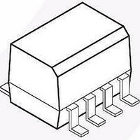
FL7930BM Fairchild Semiconductor, FL7930BM Datasheet - Page 16

FL7930BM
Manufacturer Part Number
FL7930BM
Description
Power Factor Correction ICs PFC Controller for Lighting; 2nd OVP
Manufacturer
Fairchild Semiconductor
Datasheet
1.FL7930BM.pdf
(20 pages)
Specifications of FL7930BM
Switching Frequency
300 KHz
Maximum Operating Temperature
+ 125 C
Mounting Style
SMD/SMT
Package / Case
SOP-8
Minimum Operating Temperature
- 40 C
Lead Free Status / Rohs Status
Lead free / RoHS Compliant
© 2011 Fairchild Semiconductor Corporation
FL7930 • Rev. 1.0.0
9. Startup without Overshoot: Feedback control
speed of PFC is quite slow. Due to the slow response,
there is a gap between output voltage and feedback
control. That is why over-voltage protection (OVP) is
critical at the PFC controller and voltage dip caused by
fast load changes from light to heavy is diminished by a
bulk capacitor. OVP is easily triggered during startup
phase. Operation on and off by OVP at startup may
cause audible noise and can increase voltage stress at
startup, which is normally higher than in normal
operation. This operation is better when soft-start time is
very long; however, too much startup time enlarges the
output voltage building time at light load. FL7930 has
less overshoot prevention at startup. During startup, the
feedback loop is controlled by an internal proportional
gain controller. When the output voltage reaches the
rated value, it switches to an external compensator after
a transition time of 30ms. In short, an internal
proportional gain controller eliminates overshoot at
startup and an external conventional compensator takes
over successfully afterward.
10. THD Optimization: Total Harmonic Distortion (THD)
is the factor that dictates how closely the input current
shape matches sinusoidal form. The turn-on time of the
PFC controller is almost constant over one AC line
period due to the extremely low feedback control
response. The turn-off time is determined by the current
decrease slope of the boost inductor made by the input
voltage and output voltage. Once inductor current
becomes zero, resonance between C
inductor makes oscillating waveforms at the drain pin
and auxiliary winding. By checking the auxiliary winding
voltage through the ZCD pin, the controller can check
the zero current of the boost inductor. At the same time,
a minor delay is inserted to determine the valley position
of drain voltage. The input and output voltage difference
is at its maximum at the zero-cross point of the AC input
voltage. The current decrease slope is steep near the
zero-cross region and more negative inductor current
flows during a drain voltage valley-detection time. Such
a negative inductor current cancels down the positive
current flows and input current becomes zero, called
“zero-cross distortion” in PFC.
Figure 41. Startup with Overshoot Prevention
OSS
and the boost
16
To improve this, lengthened turn-on time near the zero-
cross region is a well-known technique, though the
method may be different from company to company and
may be proprietary. FL7930 accomplishes this by
sourcing current through the ZCD pin. Auxiliary winding
voltage becomes negative when the MOSFET turns on
and is proportional to input voltage. The negative
clamping circuit of ZCD outputs the current to maintain
the ZCD voltage at a fixed value. The sourcing current
from the ZCD is directly proportional to the input
voltage. Some portion of this current is applied to the
internal sawtooth generator, together with a fixed-
current source. Theoretically, the fixed-current source
and the capacitor at sawtooth generator decide the
maximum turn-on time when no current is sourcing at
ZCD clamp circuit and available turn-on time gets
shorter proportional to the ZCD sourcing current.
Figure 42. Input and Output Current Near Input
Figure 43. Input and Output Current Near Input
Voltage Peak Zero Cross
Voltage Peak
www.fairchildsemi.com


