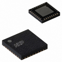
SC16C850VIBS,128 NXP Semiconductors, SC16C850VIBS,128 Datasheet - Page 32

SC16C850VIBS,128
Manufacturer Part Number
SC16C850VIBS,128
Description
IC UART SINGLE W/FIFO 32-HVQFN
Manufacturer
NXP Semiconductors
Datasheet
1.SC16C850VIBS128.pdf
(48 pages)
Specifications of SC16C850VIBS,128
Features
Programmable
Number Of Channels
1, UART
Fifo's
128 Byte
Protocol
RS485
Voltage - Supply
1.8V
With Auto Flow Control
Yes
With Irda Encoder/decoder
Yes
With False Start Bit Detection
Yes
With Modem Control
Yes
With Cmos
Yes
Mounting Type
Surface Mount
Package / Case
32-VFQFN Exposed Pad
Transmitter And Receiver Fifo Counter
Yes
Data Rate
5Mbps
Mounting
Surface Mount
Pin Count
32
Operating Temperature (min)
-40C
Operating Temperature (max)
85C
Operating Temperature Classification
Industrial
Lead Free Status / RoHS Status
Lead free / RoHS Compliant
Other names
935283087128
SC16C850VIBS-F
SC16C850VIBS-F
SC16C850VIBS-F
SC16C850VIBS-F
NXP Semiconductors
SC16C850V
Product data sheet
7.20 RS-485 turn-around time delay (RS485TIME)
7.21 Advanced Feature Control Register 1 (AFCR1)
The value in this register controls the turn-around time of the external line transceiver in
bit time. In automatic 9-bit mode, the RTS or DTR pin is used to control the direction of the
line driver, after the last bit of data has been shifted out of the transmit shift register the
UART will count down the value in this register. When the count value reaches zero, the
UART will assert the RTS or DTR pin (logic 0) to turn the external RS-485 transceiver
around for receiving.
Table 30.
Table 31.
[1]
Bit
7:0
Bit
7:5
4
3
2
1
0
It takes 4 XTAL1 clocks to reset the device.
RS485TIME[7:0] External RS-485 transceiver turn-around time delay. The value
Symbol
Symbol
AFCR1[7:5]
AFCR1[4]
AFCR1[3]
AFCR1[2]
AFCR1[1]
AFCR1[0]
RS-485 programmable turn-around time register
Advanced Feature Control Register 1 bits description
Single UART with 128-byte FIFOs, IrDA, and XScale VLIO bus interface
All information provided in this document is subject to legal disclaimers.
Sleep RXlow. Program RX input to be edge-sensitive or level-sensitive.
RTS/CTS mapped to DTR/DSR. Switch the function of RTS/CTS to
SReset. Software reset. A write to this bit will reset the UART. Once the
Description
reserved
reserved
DTR/DSR.
UART is reset this bit is automatically set to logic 0.
TSR interrupt. Select TSR interrupt mode.
Rev. 5 — 19 January 2011
logic 0 = RX input is level sensitive. If RX pin is LOW, the UART will not
go to sleep. Once the UART is in Sleep mode, it will wake up if RX pin
goes LOW.
logic 1 = RX input is edge sensitive. UART will go to sleep even if RX pin
is LOW, and will wake up when RX pin toggles.
logic 0 = RTS and CTS signals are used for hardware flow control
logic 1 = DTR and DSR signals are used for hardware flow control. RTS
and CTS retain their functionality.
logic 0 = transmit empty interrupt occurs when transmit FIFO falls below
the trigger level or becomes empty.
logic 1 = transmit empty interrupt occurs when transmit FIFO fall below
the trigger level, or becomes empty and the last stop bit has been shift
out the transmit shift register.
Description
represents the bit time at the programmed baud rate.
SC16C850V
[1]
© NXP B.V. 2011. All rights reserved.
32 of 48


