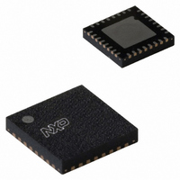
SC16C850VIBS,128 NXP Semiconductors, SC16C850VIBS,128 Datasheet - Page 5

SC16C850VIBS,128
Manufacturer Part Number
SC16C850VIBS,128
Description
IC UART SINGLE W/FIFO 32-HVQFN
Manufacturer
NXP Semiconductors
Datasheet
1.SC16C850VIBS128.pdf
(48 pages)
Specifications of SC16C850VIBS,128
Features
Programmable
Number Of Channels
1, UART
Fifo's
128 Byte
Protocol
RS485
Voltage - Supply
1.8V
With Auto Flow Control
Yes
With Irda Encoder/decoder
Yes
With False Start Bit Detection
Yes
With Modem Control
Yes
With Cmos
Yes
Mounting Type
Surface Mount
Package / Case
32-VFQFN Exposed Pad
Transmitter And Receiver Fifo Counter
Yes
Data Rate
5Mbps
Mounting
Surface Mount
Pin Count
32
Operating Temperature (min)
-40C
Operating Temperature (max)
85C
Operating Temperature Classification
Industrial
Lead Free Status / RoHS Status
Lead free / RoHS Compliant
Other names
935283087128
SC16C850VIBS-F
SC16C850VIBS-F
SC16C850VIBS-F
SC16C850VIBS-F
NXP Semiconductors
Table 2.
[1]
SC16C850V
Product data sheet
Symbol
INT
IOR
IOW
LLA
LOWPWR 9
n.c.
RESET
RI
RTS
RX
TX
V
V
XTAL1
XTAL2
DD
SS
HVQFN32 package die supply ground is connected to both V
ground for proper device operation. For enhanced thermal, electrical, and board level performance, the exposed pad needs to be
soldered to the board using a corresponding thermal pad on the board and for proper heat conduction through the board, thermal vias
need to be incorporated in the printed-circuit board in the thermal pad region.
Pin description
Pin
20
14
12
19
2, 15, 16,
17, 18
23
27
21
6
7
28
13
10
11
[1]
Type
O
I
I
I
I
-
I
I
O
I
O
I
I
I
O
…continued
Description
Interrupt output. The output state is defined by the user through the software setting of
MCR[5]. INT is set to the active mode when MCR[5] is set to a logic 0. INT is set to the
open-source mode when MCR[3] is set to a logic 1. See
Read strobe (active LOW). A HIGH to LOW transition on this signal starts the read cycle.
The SC16C850V reads a byte from the internal register and puts the byte on the data bus
for the host to retrieve.
Write strobe (active LOW). A HIGH to LOW transition on this signal starts the write cycle,
and a LOW to HIGH transition transfers the data on the data bus to the internal register.
Latch Lower Address (active LOW). A logic LOW on this pin puts the VLIO interface in the
address phase of the transaction, where the lower 8 bits of the VLIO (specifying the UART
register and the channel address) are loaded into the address latch of the device through
the AD7 to AD0 bus. A logic HIGH puts the VLIO interface in the data phase where data can
are transferred between the host and the UART.
Low Power. When asserted (active HIGH), the device immediately goes into low-power
mode. The oscillator is shut-off and some host interface pins are isolated from the host’s bus
to reduce power consumption. The device only returns to normal mode when the LOWPWR
pin is de-asserted. On the negative edge of a de-asserting LOWPWR signal, the device is
automatically reset and all registers return to their default reset states. This pin has an
internal pull-down resistor, therefore, it can be left unconnected.
not connected
Master reset (active LOW). A reset pulse will reset the internal registers and all the outputs.
The SC16C850V transmitter outputs and receiver inputs will be disabled during reset time.
(See
details.)
Ring Indicator (active LOW). A logic 0 on this pin indicates the modem has received a
ringing signal from the telephone line. A logic 1 transition on this input pin will generate an
interrupt is modem status interrupt is enabled. Status can be tested by reading MCR[6].
Request to Send (active LOW). A logic 0 on the RTS pin indicates the transmitter has data
ready and waiting to send. Writing a logic 1 in the modem control register MCR[1] will set
this pin to a logic 0, indicating data is available. After a reset this pin will be set to a logic 1.
UART receive data. The RX signal will be a logic 1 during reset, idle (no data), or when not
receiving data. During the local Loopback mode, the RX input pin is disabled and TX data is
connected to the UART RX input internally.
UART transmit data. The TX signal will be a logic 1 during reset, idle (no data), or when the
transmitter is disabled. During the local Loopback mode, the TX output pin is disabled and
TX data is internally connected to the UART RX input.
Power supply input.
Signal and power ground.
Crystal or external clock input. Functions as a crystal input or as an external clock input. A
crystal can be connected between this pin and XTAL2 to form an internal oscillator circuit.
Alternatively, an external clock can be connected to this pin to provide custom data rates
(see
Output of the crystal oscillator or buffered clock. Crystal oscillator output or buffered
clock output. Should be left open if an external clock is connected to XTAL1.
Section 6.9 “Programmable baud rate
Section 7.23 “SC16C850V external reset condition and software reset”
Single UART with 128-byte FIFOs, IrDA, and XScale VLIO bus interface
All information provided in this document is subject to legal disclaimers.
Rev. 5 — 19 January 2011
SS
pin and exposed center pad. V
generator”). See
Table
SS
pin must be connected to supply
Figure
19.
SC16C850V
4.
© NXP B.V. 2011. All rights reserved.
for initialization
5 of 48


