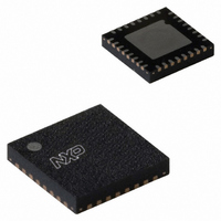
SC16C850VIBS,128 NXP Semiconductors, SC16C850VIBS,128 Datasheet - Page 8

SC16C850VIBS,128
Manufacturer Part Number
SC16C850VIBS,128
Description
IC UART SINGLE W/FIFO 32-HVQFN
Manufacturer
NXP Semiconductors
Datasheet
1.SC16C850VIBS128.pdf
(48 pages)
Specifications of SC16C850VIBS,128
Features
Programmable
Number Of Channels
1, UART
Fifo's
128 Byte
Protocol
RS485
Voltage - Supply
1.8V
With Auto Flow Control
Yes
With Irda Encoder/decoder
Yes
With False Start Bit Detection
Yes
With Modem Control
Yes
With Cmos
Yes
Mounting Type
Surface Mount
Package / Case
32-VFQFN Exposed Pad
Transmitter And Receiver Fifo Counter
Yes
Data Rate
5Mbps
Mounting
Surface Mount
Pin Count
32
Operating Temperature (min)
-40C
Operating Temperature (max)
85C
Operating Temperature Classification
Industrial
Lead Free Status / RoHS Status
Lead free / RoHS Compliant
Other names
935283087128
SC16C850VIBS-F
SC16C850VIBS-F
SC16C850VIBS-F
SC16C850VIBS-F
NXP Semiconductors
SC16C850V
Product data sheet
6.4.1 32-byte FIFO mode
6.4.2 128-byte FIFO mode
6.4 FIFO operation
6.5 Hardware flow control
[3]
[4]
[5]
[6]
When all four of these registers (TXINTLVL, RXINTLVL, FLWCNTH, FLWCNTL) in the
First Extra Register Set are empty (0x00) the transmit and receive trigger levels are set by
FCR[7:4]. In this mode the transmit and receive trigger levels are backward compatible to
the SC16C650B (see
receive data FIFOs are enabled by the FIFO Control Register bit 0 (FCR[0]). It should be
noted that the user can set the transmit trigger levels by writing to the FCR, but activation
will not take place until EFR[4] is set to a logic 1. The receiver FIFO section includes a
time-out function to ensure data is delivered to the external CPU (see
refer to
Table 5.
When either TXINTLVL, RXINTLVL, FLWCNTH or FLWCNTL in the First Extra Register
Set contains any value other than 0x00, the transmit and receive trigger levels are set by
TXINTLVL and RXINTLVL registers. TXINTLVL sets the trigger levels for the transmit
FIFO, and the transmit trigger levels can be set to any value between 1 and 128 with
granularity of 1. RXINTLVL sets the trigger levels for the receive FIFO, the receive trigger
levels can be set to any value between 1 and 128 with granularity of 1.
When the effective FIFO size changes (that is, when FCR[0] toggles or when the
combined content of TXINTLVL, RXINTLVL, FLWCNTH and FLWCNTL changes between
equal and unequal to 0x00), both RX FIFO and TX FIFO will be reset (data in the FIFO will
be lost).
When automatic hardware flow control is enabled, the SC16C850V monitors the CTS pin
for a remote buffer overflow indication and controls the RTS pin for local buffer overflows.
Automatic hardware flow control is selected by setting EFR[6] (RTS) and EFR[7] (CTS) to
a logic 1. If CTS transitions from a logic 0 to a logic 1 indicating a flow control request,
ISR[5] will be set to a logic 1 (if enabled via IER[7:6]), and the SC16C850V will suspend
TX transmissions as soon as the stop bit of the character in process is shifted out.
Transmission is resumed after the CTS input returns to a logic 0, indicating more data
may be sent.
FCR[7:6]
00
01
10
11
Second special registers are accessible only when EFCR[0] = 1.
Enhanced Feature Registers are only accessible when LCR = 0xBF.
First extra feature registers are only accessible when EFCR[2:1] = 01b.
Second extra feature registers are only accessible when EFCR[2:1] = 10b.
Table 10
Interrupt trigger level and Flow control mechanism
Single UART with 128-byte FIFOs, IrDA, and XScale VLIO bus interface
FCR[5:4]
00
01
10
11
All information provided in this document is subject to legal disclaimers.
and
Table 11
Table
Rev. 5 — 19 January 2011
5), and the FIFO sizes are 32 entries. The transmit and
8
16
24
28
INT pin activation
RX
for the setting of FCR[7:4].
TX
16
8
24
30
Negate RTS or
send Xoff
8
16
24
28
SC16C850V
Section
© NXP B.V. 2011. All rights reserved.
Assert RTS
or send Xon
0
7
15
23
6.8). Please
8 of 48


