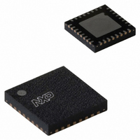
SC16C850VIBS,128 NXP Semiconductors, SC16C850VIBS,128 Datasheet - Page 4

SC16C850VIBS,128
Manufacturer Part Number
SC16C850VIBS,128
Description
IC UART SINGLE W/FIFO 32-HVQFN
Manufacturer
NXP Semiconductors
Datasheet
1.SC16C850VIBS128.pdf
(48 pages)
Specifications of SC16C850VIBS,128
Features
Programmable
Number Of Channels
1, UART
Fifo's
128 Byte
Protocol
RS485
Voltage - Supply
1.8V
With Auto Flow Control
Yes
With Irda Encoder/decoder
Yes
With False Start Bit Detection
Yes
With Modem Control
Yes
With Cmos
Yes
Mounting Type
Surface Mount
Package / Case
32-VFQFN Exposed Pad
Transmitter And Receiver Fifo Counter
Yes
Data Rate
5Mbps
Mounting
Surface Mount
Pin Count
32
Operating Temperature (min)
-40C
Operating Temperature (max)
85C
Operating Temperature Classification
Industrial
Lead Free Status / RoHS Status
Lead free / RoHS Compliant
Other names
935283087128
SC16C850VIBS-F
SC16C850VIBS-F
SC16C850VIBS-F
SC16C850VIBS-F
NXP Semiconductors
5. Pinning information
Table 2.
SC16C850V
Product data sheet
Symbol
AD0
AD1
AD2
AD3
AD4
AD5
AD6
AD7
CD
CS
CTS
DSR
DTR
Pin description
Pin
29
30
31
32
1
3
4
5
26
8
24
25
22
5.1 Pinning
5.2 Pin description
Type
I/O
I
I
I
I
O
Fig 2.
Description
Address and Data bus (bidirectional). These pins are the 8-bit multiplexed data bus and
address bus for transferring information to or from the controlling CPU. AD0 is the least
significant bit and is address A0 during the address cycle, and AD7 is the most significant bit
and is address A7 during the address cycle.
Carrier Detect (active LOW). A logic 0 on this pin indicates that a carrier has been detected
by the modem for that channel. Status can be tested by reading MSR[7].
Chip Select (active LOW). This pin enables the data transfers between the host and the
SC16C850V.
Clear to Send (active LOW). A logic 0 on the CTS pin indicates the modem or data set is
ready to accept transmit data from the SC16C850V. Status can be tested by reading
MSR[4].
Data Set Ready (active LOW). A logic 0 on this pin indicates the modem or data set is
powered-on and is ready for data exchange with the UART. Status can be tested by reading
MSR[5].
Data Terminal Ready (active LOW). A logic 0 on this pin indicates that the SC16C850V is
powered-on and ready. This pin can be controlled via the Modem Control Register. Writing a
logic 1 to MCR[0] will set the DTR output to logic 0, enabling the modem. This pin will be a
logic 1 after writing a logic 0 to MCR[0], or after a reset.
Pin configuration for HVQFN32
Single UART with 128-byte FIFOs, IrDA, and XScale VLIO bus interface
All information provided in this document is subject to legal disclaimers.
Rev. 5 — 19 January 2011
index area
terminal 1
AD4
AD5
AD6
AD7
n.c.
RX
CS
TX
1
2
3
4
5
6
7
8
Transparent top view
SC16C850VIBS
24
23
22
21
20
19
18
17
002aac557
CTS
RESET
DTR
RTS
INT
LLA
n.c.
n.c.
SC16C850V
© NXP B.V. 2011. All rights reserved.
4 of 48


