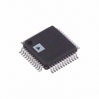
ADAU1701JSTZ Analog Devices Inc, ADAU1701JSTZ Datasheet - Page 12

ADAU1701JSTZ
Manufacturer Part Number
ADAU1701JSTZ
Description
IC AUDIO PROC 2ADC/4DAC 48-LQFP
Manufacturer
Analog Devices Inc
Series
SigmaDSP®r
Type
Audio Processorr
Specifications of ADAU1701JSTZ
Design Resources
Analog Audio Input, Class-D Output with ADAU1701, SSM2306, and ADP3336 (CN0162)
Applications
Automotive, Monitors, MP3
Mounting Type
Surface Mount
Package / Case
48-LQFP
Audio Control Type
Digital
Control Interface
I2C, Serial
Supply Voltage Range
1.8V, 3.3V
Operating Temperature Range
0°C To +70°C
Audio Ic Case Style
LQFP
No. Of Pins
48
Svhc
No SVHC
Control / Process Application
MP3 Player Speaker Docks, Automotive Head Units, Studio Monitors
Rohs Compliant
Yes
Lead Free Status / RoHS Status
Lead free / RoHS Compliant
For Use With
EVAL-ADAU1701MINIZ - BOARD EVAL SIGMADSP AUD ADAU1701EVAL-ADAU1701EBZ - BOARD EVAL FOR ADAU1701
Lead Free Status / RoHS Status
Lead free / RoHS Compliant, Lead free / RoHS Compliant
Available stocks
Company
Part Number
Manufacturer
Quantity
Price
Company:
Part Number:
ADAU1701JSTZ
Manufacturer:
Analog Devices Inc
Quantity:
1 923
Company:
Part Number:
ADAU1701JSTZ
Manufacturer:
ADI
Quantity:
221
Company:
Part Number:
ADAU1701JSTZ
Manufacturer:
Analog Devices Inc
Quantity:
10 000
Part Number:
ADAU1701JSTZ
Manufacturer:
ADI/亚德诺
Quantity:
20 000
Company:
Part Number:
ADAU1701JSTZ-RL
Manufacturer:
ON
Quantity:
35 000
Company:
Part Number:
ADAU1701JSTZ-RL
Manufacturer:
Analog Devices Inc
Quantity:
10 000
Part Number:
ADAU1701JSTZ-RL
Manufacturer:
ADI/亚德诺
Quantity:
20 000
ADAU1701
PIN CONFIGURATION AND FUNCTION DESCRIPTIONS
Table 11. Pin Function Descriptions
Pin No.
1, 37, 42
2
3
4
5
6
7
8
9
10
11
12, 25
13, 24
Mnemonic
AGND
ADC0
ADC_RES
ADC1
RESET
SELFBOOT
ADDR0
MP4
MP5
MP1
MP0
DGND
DVDD
Type
PWR
A_IN
A_IN
A_IN
D_IN
D_IN
D_IN
D_IO
D_IO
D_IO
D_IO
PWR
PWR
1
SELFBOOT
ADC_RES
ADDR0
RESET
AGND
DGND
ADC0
ADC1
MP4
MP5
MP1
MP0
Description
Analog Ground Pin. The AGND, DGND, and PGND pins can be tied directly together in a
common ground plane. Decouple AGND to an AVDD pin with a 100 nF capacitor.
Analog Audio Input 0. Full-scale 100 μA rms input. Current input allows input voltage level
to be scaled with an external resistor. An 18 kΩ resistor gives a 2 V rms full-scale input. See
the Audio ADCs section for details.
ADC Reference Current. Set the full-scale current of the ADCs with an external 18 kΩ resistor
connected between this pin and ground. See the Audio ADCs section for details.
Analog Audio Input 1. Full-scale 100 μA rms input. Current input allows the input voltage
level to be scaled with an external resistor. An 18 kΩ resistor gives a 2 V rms full-scale input.
Active Low Reset Input. Reset is triggered on a high-to-low edge, and the ADAU1701 exits
reset on a low-to-high edge. For more information about initialization, see the Power-Up
Sequence section for details.
Enable/Disable Self-Boot. SELFBOOT selects control port (low) or self-boot (high). Setting
this pin high initiates a self-boot operation when the ADAU1701 is brought out of a reset. This
pin can be tied directly to the control voltage or pulled up/down with a resistor. See the
Self-Boot section for details.
I
four ADAU1701 devices to be used on the same I
common SPI CLATCH signal. See the I
Multipurpose GPIO or Serial Input Port LRCLK (INPUT_LRCLK). See the Multipurpose Pins
section for more details.
Multipurpose GPIO or Serial Input Port BCLK (INPUT_BCLK). See the Multipurpose Pins
section for more details.
Multipurpose GPIO or Serial Input Port Data 1 (SDATA_IN0). See the Multipurpose Pins
section for more details.
Multipurpose GPIO or Serial Input Port Data 0 (SDATA_IN1). See the Multipurpose Pins
section for more details.
Digital Ground Pin. The AGND, DGND, and PGND pins can be tied directly together in a
common ground plane. Decouple DGND to a DVDD pin with a 100 nF capacitor.
1.8 V Digital Supply. This can be supplied either externally or generated from a 3.3 V supply
with the on-board 1.8 V regulator. Decouple DVDD to DGND with a 100 nF capacitor.
2
C and SPI Address 0. In combination with ADDR1 function on Pin 20, this pin allows up to
10
11
12
Figure 7. 48-Lead LQFP Pin Configuration
1
2
3
4
5
6
7
8
9
48 47 46 45 44 43 42 41 40 39 38 37
13 14 15 16 17 18 19 20 21 22 23 24
PIN 1
INDICATOR
Rev. A | Page 12 of 56
ADAU1701
(Not to Scale)
TOP VIEW
2
C Port section for details.
36
35
34
33
32
31
30
29
28
26
25
27
AVDD
PLL_LF
PVDD
PGND
MCLKI
OSCO
RSVD
MP2
MP3
MP8
MP9
DGND
2
C bus and up to two ICs to be used with a


