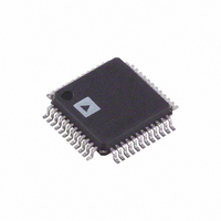
ADAU1701JSTZ Analog Devices Inc, ADAU1701JSTZ Datasheet - Page 47

ADAU1701JSTZ
Manufacturer Part Number
ADAU1701JSTZ
Description
IC AUDIO PROC 2ADC/4DAC 48-LQFP
Manufacturer
Analog Devices Inc
Series
SigmaDSP®r
Type
Audio Processorr
Specifications of ADAU1701JSTZ
Design Resources
Analog Audio Input, Class-D Output with ADAU1701, SSM2306, and ADP3336 (CN0162)
Applications
Automotive, Monitors, MP3
Mounting Type
Surface Mount
Package / Case
48-LQFP
Audio Control Type
Digital
Control Interface
I2C, Serial
Supply Voltage Range
1.8V, 3.3V
Operating Temperature Range
0°C To +70°C
Audio Ic Case Style
LQFP
No. Of Pins
48
Svhc
No SVHC
Control / Process Application
MP3 Player Speaker Docks, Automotive Head Units, Studio Monitors
Rohs Compliant
Yes
Lead Free Status / RoHS Status
Lead free / RoHS Compliant
For Use With
EVAL-ADAU1701MINIZ - BOARD EVAL SIGMADSP AUD ADAU1701EVAL-ADAU1701EBZ - BOARD EVAL FOR ADAU1701
Lead Free Status / RoHS Status
Lead free / RoHS Compliant, Lead free / RoHS Compliant
Available stocks
Company
Part Number
Manufacturer
Quantity
Price
Company:
Part Number:
ADAU1701JSTZ
Manufacturer:
Analog Devices Inc
Quantity:
1 923
Company:
Part Number:
ADAU1701JSTZ
Manufacturer:
ADI
Quantity:
221
Company:
Part Number:
ADAU1701JSTZ
Manufacturer:
Analog Devices Inc
Quantity:
10 000
Part Number:
ADAU1701JSTZ
Manufacturer:
ADI/亚德诺
Quantity:
20 000
Company:
Part Number:
ADAU1701JSTZ-RL
Manufacturer:
ON
Quantity:
35 000
Company:
Part Number:
ADAU1701JSTZ-RL
Manufacturer:
Analog Devices Inc
Quantity:
10 000
Part Number:
ADAU1701JSTZ-RL
Manufacturer:
ADI/亚德诺
Quantity:
20 000
The serial data clocks need to be synchronous with the ADAU1701
master clock input.
The input control register allows control of clock polarity and
data input modes. The valid data formats are I
right-justified (24-/20-/18-/16-bit), and 8-channel TDM. In all
modes except for the right-justified modes, the serial port accepts
an arbitrary number of bits up to a limit of 24. Extra bits do not
cause an error, but they are truncated internally. Proper operation
of the right-justified modes requires that there be exactly 64 BCLKs
per audio frame. The TDM data is input on SDATA_IN0. The
LRCLK in TDM mode can be input to the ADAU1701 either as
a 50/50 duty cycle clock or as a bit-wide pulse.
In TDM mode, the ADAU1701 can be a master for 48 kHz and
96 kHz data, but not for 192 kHz data. Table 64 lists the modes
in which the serial output port can function.
Table 64. Serial Output Port Master/Slave Mode Capabilities
f
48 kHz
96 kHz
192 kHz
The output control registers allow the user to control clock
polarities, clock frequencies, clock types, and data format. In all
modes except for the right-justified modes (MSB delayed by 8,
12, or 16 bits), the serial port accepts an arbitrary number of
bits up to a limit of 24. Extra bits do not cause an error, but are
truncated internally. Proper operation of the right-justified modes
requires the LSB to align with the edge of the LRCLK. The default
settings of all serial port control registers correspond to 2-channel
I
modes unless otherwise noted.
The function of each multipurpose pin in serial data port mode
is shown in Table 65. Pin MP0 to Pin MP5 support digital data
input to the ADAU1701, and Pin MP6 to Pin MP11 handle digital
data output from the DSP. The configuration of the serial data
Table 66. Data Format Configurations
Format
I
Left-Justified (Figure 33)
Right-Justified (Figure 34)
TDM with Clock (Figure 35)
TDM with Pulse (Figure 36)
2
S
2
S (Figure 32)
S mode. All register settings apply to both master and slave
2-Channel Modes
(I
Right Justified)
Master and slave
Master and slave
Master and slave
2
S, Left Justified,
LRCLK Polarity
Frame begins on falling edge
Frame begins on rising edge
Frame begins on rising edge
Frame begins on falling edge
Frame begins on rising edge
8-Channel TDM
Master and slave
Master and slave
Slave only
2
S, left-justified,
Rev. A | Page 47 of 56
LRCLK
Type
Clock
Clock
Clock
Clock
Pulse
BCLK Polarity
Data changes on falling edge
Data changes on falling edge
Data changes on falling edge
Data changes on falling edge
Data changes on falling edge
input port is set in the serial input control register (Table 51), and
the configuration of the corresponding output port is controlled
with the serial output control register (Table 49). The clocks of
the input port function only as slaves, whereas the output port
clocks can be set to function as either masters or slaves. The
INPUT_LRCLK (MP4) and INPUT_BCLK (MP5) pins are
used to clock the SDATA_INx (MP0 to MP3) signals, and the
OUTPUT_LRCLK (MP10) and OUTPUT_BCLK (MP11) pins
are used to clock the SDATA_OUTx (MP6 to MP9) signals.
If an external ADC is connected as a slave to the ADAU1701,
use both the input and output port clocks. The OUTPUT_LRCLK
(MP10) and OUTPUT_BCLK (MP11) pins must be set to master
mode and connected externally to the INPUT_LRCLK (MP4)
and INPUT_BCLK (MP5) pins as well as to the external ADC
clock input pins. The data is output from the external ADC into
the SigmaDSP on one of the four SDATA_INx pins (MP0 to MP3).
Connections to an external DAC are handled exclusively with the
output port pins. The OUTPUT_LRCLK and OUTPUT_BCLK
pins can be set to function as either masters or slaves, and the
SDATA_OUTx pins are used to output data from the SigmaDSP
to the external DAC.
Table 66 describes the proper configurations for standard audio
data formats.
Table 65. Multipurpose Pin Serial Data Port Functions
Multipurpose Pin
MP0
MP1
MP2
MP3
MP4
MP5
MP6
MP7
MP8
MP9
MP10
MP11
Function
SDATA_IN0/TDM_IN
SDATA_IN1
SDATA_IN2
SDATA_IN3
INPUT_LRCLK (slave only)
INPUT_BCLK (slave only)
SDATA_OUT0/TDM_OUT
SDATA_OUT1
SDATA_OUT2
SDATA_OUT3
OUTPUT_LRCLK (master or slave)
OUTPUT_BCLK (master or slave)
MSB Position
Delayed from LRCLK edge
by 1 BCLK
Aligned with LRCLK edge
Delayed from LRCLK edge
by 8, 12, or 16 BCLKs
Delayed from start of word clock
by 1 BCLK
Delayed from start of word clock
by 1 BCLK
ADAU1701


