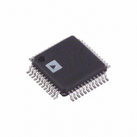
ADAU1701JSTZ Analog Devices Inc, ADAU1701JSTZ Datasheet - Page 26

ADAU1701JSTZ
Manufacturer Part Number
ADAU1701JSTZ
Description
IC AUDIO PROC 2ADC/4DAC 48-LQFP
Manufacturer
Analog Devices Inc
Series
SigmaDSP®r
Type
Audio Processorr
Specifications of ADAU1701JSTZ
Design Resources
Analog Audio Input, Class-D Output with ADAU1701, SSM2306, and ADP3336 (CN0162)
Applications
Automotive, Monitors, MP3
Mounting Type
Surface Mount
Package / Case
48-LQFP
Audio Control Type
Digital
Control Interface
I2C, Serial
Supply Voltage Range
1.8V, 3.3V
Operating Temperature Range
0°C To +70°C
Audio Ic Case Style
LQFP
No. Of Pins
48
Svhc
No SVHC
Control / Process Application
MP3 Player Speaker Docks, Automotive Head Units, Studio Monitors
Rohs Compliant
Yes
Lead Free Status / RoHS Status
Lead free / RoHS Compliant
For Use With
EVAL-ADAU1701MINIZ - BOARD EVAL SIGMADSP AUD ADAU1701EVAL-ADAU1701EBZ - BOARD EVAL FOR ADAU1701
Lead Free Status / RoHS Status
Lead free / RoHS Compliant, Lead free / RoHS Compliant
Available stocks
Company
Part Number
Manufacturer
Quantity
Price
Company:
Part Number:
ADAU1701JSTZ
Manufacturer:
Analog Devices Inc
Quantity:
1 923
Company:
Part Number:
ADAU1701JSTZ
Manufacturer:
ADI
Quantity:
221
Company:
Part Number:
ADAU1701JSTZ
Manufacturer:
Analog Devices Inc
Quantity:
10 000
Part Number:
ADAU1701JSTZ
Manufacturer:
ADI/亚德诺
Quantity:
20 000
Company:
Part Number:
ADAU1701JSTZ-RL
Manufacturer:
ON
Quantity:
35 000
Company:
Part Number:
ADAU1701JSTZ-RL
Manufacturer:
Analog Devices Inc
Quantity:
10 000
Part Number:
ADAU1701JSTZ-RL
Manufacturer:
ADI/亚德诺
Quantity:
20 000
ADAU1701
I
Figure 22 shows the timing of a single-word write operation.
Every ninth clock, the ADAU1701 issues an acknowledge by
pulling SDA low.
Figure 23 shows the timing of a burst mode write sequence.
This figure shows an example where the target destination
registers are two bytes. The ADAU1701 knows to increment
its subaddress register every two bytes because the requested
subaddress corresponds to a register or memory area with a
2-byte word length.
The timing of a single-word read operation is shown in
Figure 24. Note that the first R/ W bit is 0, indicating a write
operation. This is because the subaddress still needs to be
written to set up the internal address. After the ADAU1701
acknowledges the receipt of the subaddress, the master must
issue a repeated start command followed by the chip address
byte with the R/ W set to 1 (read). This causes the ADAU1701
SDA to reverse and begin driving data back to the master. The
2
C Read and Write Operations
S
S
S
S
CHIP ADDRESS,
CHIP ADDRESS,
CHIP ADDRESS,
CHIP ADDRESS,
R/W = 0
R/W = 0
R/W = 0
R/W = 0
AS
AS
AS
AS
SUBADDRESS
SUBADDRESS
SUBADDRESS
SUBADDRESS
HIGH
HIGH
HIGH
HIGH
AS
AS
AS
AS
SUBADDRESS
SUBADDRESS
SUBADDRESS
LOW
SUBADDRESS
LOW
Figure 22. Single Word I
Figure 24. Single-Word I
Figure 23. Burst Mode I
Figure 25. Burst Mode I
LOW
LOW
AS
Rev. A | Page 26 of 56
AS
AS
S
AS
WORD 1,
BYTE 1
DATA-
CHIP ADDRESS,
S
DATA BYTE 1
R/W = 1
CHIP ADDRESS,
2
2
2
2
C Write Format
C Read Format
C Write Format
C Read Format
master then responds every ninth pulse with an acknowledge
pulse to the ADAU1701.
Figure 25 shows the timing of a burst mode read sequence. This
figure shows an example where the target read registers are two
bytes. The ADAU1701 increments its subaddress every two bytes
because the requested subaddress corresponds to a register or
memory area with word lengths of two bytes. Other addresses
may have word lengths ranging from one to five bytes. The
ADAU1701 always decodes the subaddress and sets the auto-
increment circuit so that the address increments after the
appropriate number of bytes.
Figure 22 to Figure 25 use the following abbreviations:
S = start bit
P = stop bit
AM = acknowledge by master
AS = acknowledge by slave
AS
R/W = 1
WORD 1,
BYTE 2
DATA-
AS
AS
AS
BYTE 1
DATA
AS
DATA BYTE 2
WORD 1,
BYTE 1
DATA-
WORD 2,
BYTE 1
DATA-
AM
BYTE 2
AM
DATA
AS
WORD 1,
AS
BYTE 2
WORD 2,
DATA-
BYTE 2
DATA-
DATA BYTE N
AM
AM
AS
BYTE N
DATA
P
P
P
P


