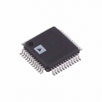
ADAU1701JSTZ Analog Devices Inc, ADAU1701JSTZ Datasheet - Page 41

ADAU1701JSTZ
Manufacturer Part Number
ADAU1701JSTZ
Description
IC AUDIO PROC 2ADC/4DAC 48-LQFP
Manufacturer
Analog Devices Inc
Series
SigmaDSP®r
Type
Audio Processorr
Specifications of ADAU1701JSTZ
Design Resources
Analog Audio Input, Class-D Output with ADAU1701, SSM2306, and ADP3336 (CN0162)
Applications
Automotive, Monitors, MP3
Mounting Type
Surface Mount
Package / Case
48-LQFP
Audio Control Type
Digital
Control Interface
I2C, Serial
Supply Voltage Range
1.8V, 3.3V
Operating Temperature Range
0°C To +70°C
Audio Ic Case Style
LQFP
No. Of Pins
48
Svhc
No SVHC
Control / Process Application
MP3 Player Speaker Docks, Automotive Head Units, Studio Monitors
Rohs Compliant
Yes
Lead Free Status / RoHS Status
Lead free / RoHS Compliant
For Use With
EVAL-ADAU1701MINIZ - BOARD EVAL SIGMADSP AUD ADAU1701EVAL-ADAU1701EBZ - BOARD EVAL FOR ADAU1701
Lead Free Status / RoHS Status
Lead free / RoHS Compliant, Lead free / RoHS Compliant
Available stocks
Company
Part Number
Manufacturer
Quantity
Price
Company:
Part Number:
ADAU1701JSTZ
Manufacturer:
Analog Devices Inc
Quantity:
1 923
Company:
Part Number:
ADAU1701JSTZ
Manufacturer:
ADI
Quantity:
221
Company:
Part Number:
ADAU1701JSTZ
Manufacturer:
Analog Devices Inc
Quantity:
10 000
Part Number:
ADAU1701JSTZ
Manufacturer:
ADI/亚德诺
Quantity:
20 000
Company:
Part Number:
ADAU1701JSTZ-RL
Manufacturer:
ON
Quantity:
35 000
Company:
Part Number:
ADAU1701JSTZ-RL
Manufacturer:
Analog Devices Inc
Quantity:
10 000
Part Number:
ADAU1701JSTZ-RL
Manufacturer:
ADI/亚德诺
Quantity:
20 000
2078 (0x081E)—SERIAL OUTPUT CONTROL REGISTER
Table 48. Serial Output Control Register Bit Map
D15
0
Table 49.
Bit Name
OLRP
OBP
M/S
OBF[1:0]
OLF[1:0]
FST
TDM
MSB[2:0]
OWL[1:0]
D14
0
D13
OLRP
D12
OBP
Description
OUTPUT_LRCLK Polarity. When this bit is set to 0, the left-channel data is clocked when OUTPUT_LRCLK is
low and the right-channel data is clocked when OUTPUT_LRCLK is high. When this bit is set to 1, the right-
channel data is clocked when OUTPUT_LRCLK is low and the left-channel data is clocked when
OUTPUT_LRCLK is high.
OUTPUT_BCLK Polarity. This bit controls on which edge of the bit clock the output data is clocked. Data
changes on the falling edge of OUTPUT_BCLK when this bit is set to 0 and on the rising edge when this bit is
set to 1.
Master/Slave. This bit sets whether the output port is a clock master or slave. The default setting is slave; on
power-up, the OUTPUT_BCLK and OUTPUT_LRCLK pins are set as inputs until this bit is set to 1, at which time
they become clock outputs.
OUTPUT_BCLK Frequency (Master Mode Only). When the output port is being used as a clock master, these
bits set the frequency of the output bit clock, which is divided down from an internal 1024 × f
(49.152 MHz for a f
OBF[1:0]
00
01
10
11
OUTPUT_LRCLK Frequency (Master Mode Only). When the output port is used as a clock master, these bits set
the frequency of the output word clock on the OUTPUT_LRCLK pins, which is divided down from an internal
1024 × f
OLF[1:0]
00
01
10
11
Frame Sync Type. This bit sets the type of signal on the OUTPUT_LRCLK pins. When this bit is set to 0, the
signal is a word clock with a 50% duty cycle; when this bit is set to 1, the signal is a pulse with a duration of
one bit clock at the beginning of the data frame.
TDM Enable. Setting this bit to 1 changes the output port from four serial stereo outputs to a single
8-channel TDM output stream on the SDATA_OUT0 pin (MP6).
MSB Position. These three bits set the position of the MSB of data with respect to the LRCLK edge. The data
output of the ADAU1701 is always MSB first.
MSB[2:0]
000
001
010
011
100
101
111
Output Word Length. These bits set the word length of the output data-word. All bits following the LSB are
set to 0.
OWL[1:0]
00
01
10
11
D11
M/S
S
D10
OBF1
clock (49.152 MHz for a f
Setting
Internal clock/16
Internal clock/8
Internal clock/4
Internal clock/2
Setting
Internal clock/1024
Internal clock/512
Internal clock/256
Reserved
Setting
Delay by 1
Delay by 0
Delay by 8
Delay by 12
Delay by 16
Reserved
Reserved
Setting
24 bits
20 bits
16 bits
Reserved
D9
OBF0
S
of 48 kHz).
D8
OLF1
Rev. A | Page 41 of 56
S
of 48 kHz).
D7
OLF0
D6
FST
D5
TDM
D4
MSB2
D3
MSB1
D2
MSB0
D1
OWL1
D0
OWL0
ADAU1701
S
clock
Default
0x0000


