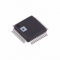
ADAU1701JSTZ Analog Devices Inc, ADAU1701JSTZ Datasheet - Page 27

ADAU1701JSTZ
Manufacturer Part Number
ADAU1701JSTZ
Description
IC AUDIO PROC 2ADC/4DAC 48-LQFP
Manufacturer
Analog Devices Inc
Series
SigmaDSP®r
Type
Audio Processorr
Specifications of ADAU1701JSTZ
Design Resources
Analog Audio Input, Class-D Output with ADAU1701, SSM2306, and ADP3336 (CN0162)
Applications
Automotive, Monitors, MP3
Mounting Type
Surface Mount
Package / Case
48-LQFP
Audio Control Type
Digital
Control Interface
I2C, Serial
Supply Voltage Range
1.8V, 3.3V
Operating Temperature Range
0°C To +70°C
Audio Ic Case Style
LQFP
No. Of Pins
48
Svhc
No SVHC
Control / Process Application
MP3 Player Speaker Docks, Automotive Head Units, Studio Monitors
Rohs Compliant
Yes
Lead Free Status / RoHS Status
Lead free / RoHS Compliant
For Use With
EVAL-ADAU1701MINIZ - BOARD EVAL SIGMADSP AUD ADAU1701EVAL-ADAU1701EBZ - BOARD EVAL FOR ADAU1701
Lead Free Status / RoHS Status
Lead free / RoHS Compliant, Lead free / RoHS Compliant
Available stocks
Company
Part Number
Manufacturer
Quantity
Price
Company:
Part Number:
ADAU1701JSTZ
Manufacturer:
Analog Devices Inc
Quantity:
1 923
Company:
Part Number:
ADAU1701JSTZ
Manufacturer:
ADI
Quantity:
221
Company:
Part Number:
ADAU1701JSTZ
Manufacturer:
Analog Devices Inc
Quantity:
10 000
Part Number:
ADAU1701JSTZ
Manufacturer:
ADI/亚德诺
Quantity:
20 000
Company:
Part Number:
ADAU1701JSTZ-RL
Manufacturer:
ON
Quantity:
35 000
Company:
Part Number:
ADAU1701JSTZ-RL
Manufacturer:
Analog Devices Inc
Quantity:
10 000
Part Number:
ADAU1701JSTZ-RL
Manufacturer:
ADI/亚德诺
Quantity:
20 000
SPI PORT
By default, the ADAU1701 is in I
SPI control mode by pulling CLATCH/WP low three times. The
SPI port uses a 4-wire interface, consisting of CLATCH, CCLK,
CDATA, and COUT signals, and is always a slave port. The
CLATCH signal should go low at the beginning of a transaction
and high at the end of a transaction. The CCLK signal latches
CDATA during a low-to-high transition. COUT data is shifted
out of the ADAU1701 on the falling edge of CCLK and should be
clocked into a receiving device, such as a microcontroller, on the
CCLK rising edge. The CDATA signal carries the serial input
data, and the COUT signal is the serial output data. The COUT
signal remains three-stated until a read operation is requested.
This allows other SPI-compatible peripherals to share the same
readback line. All SPI transactions have the same basic format
shown in Table 19. A timing diagram is shown in Figure 3. All
data should be written MSB first. The ADAU1701 cannot be
taken out of SPI mode without a full reset.
Chip Address R/ W
The first byte of an SPI transaction includes the 7-bit chip address
and a R/ W bit. The chip address is set by the ADDR0 pin. This
allows two ADAU1701s to share a CLATCH signal, yet still operate
independently. When ADDR0 is low, the chip address is 0000000;
when it is high, the address is 0000001 (see
of this first byte determines whether the SPI transaction is a
read (Logic Level 1) or a write (Logic Level 0).
Table 19. Generic Control Word Format
Byte 0
chip_adr[6:0], R/W
1
Continues to end of data.
CLATCH
CDATA
CCLK
CLATCH
CDATA
COUT
CCLK
2
C mode, but it can be put into
BYTE 0
Byte 1
0000, subadr[11:8]
HIGH-Z
BYTE 0
Figure 27. SPI Read from ADAU1701 Clocking (Single-Read Mode)
Figure 26. SPI Write to ADAU1701 Clocking (Single-Write Mode)
Table 18
BYTE 1
). The LSB
Rev. A | Page 27 of 56
Byte 2
subadr[7:0]
BYTE 2
Table 18. ADAU1701 SPI Address Byte Format
Bit 0
0
Subaddress
The 12-bit subaddress word is decoded into a location in one of
the memories or registers. This subaddress is the location of the
appropriate RAM location or register. The MSBs of the subaddress
are zero-padded to bring the word to a full 2-byte length.
Data Bytes
The number of data bytes varies according to the register or
memory being accessed. During a burst mode write, an initial
subaddress is written followed by a continuous sequence of data
for consecutive memory/register locations. The detailed data
format for continuous mode operation is shown in Table 23 and
Table 25 in the Read/Write Data Formats section.
A sample timing diagram for a single-write SPI operation to the
parameter RAM is shown in Figure 26. A sample timing diagram
of a single-read SPI operation is shown in Figure 27. The COUT
pin goes from three-state to being driven at the beginning of
Byte 3. In this example, Byte 0 to Byte 2 contain the addresses
and the R/ W bit and subsequent bytes carry the data.
BYTE 1
Bit 1
0
DATA
Bit 2
0
BYTE 2
Byte 3
data
Bit 3
0
DATA
Bit 4
0
BYTE 3
HIGH-Z
Bit 5
0
Byte 4
data
ADAU1701
Bit 6
ADDR0
1
Bit 7
R/W


