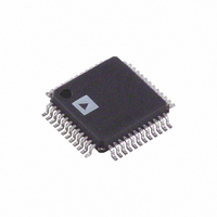
ADAU1701JSTZ Analog Devices Inc, ADAU1701JSTZ Datasheet - Page 21

ADAU1701JSTZ
Manufacturer Part Number
ADAU1701JSTZ
Description
IC AUDIO PROC 2ADC/4DAC 48-LQFP
Manufacturer
Analog Devices Inc
Series
SigmaDSP®r
Type
Audio Processorr
Specifications of ADAU1701JSTZ
Design Resources
Analog Audio Input, Class-D Output with ADAU1701, SSM2306, and ADP3336 (CN0162)
Applications
Automotive, Monitors, MP3
Mounting Type
Surface Mount
Package / Case
48-LQFP
Audio Control Type
Digital
Control Interface
I2C, Serial
Supply Voltage Range
1.8V, 3.3V
Operating Temperature Range
0°C To +70°C
Audio Ic Case Style
LQFP
No. Of Pins
48
Svhc
No SVHC
Control / Process Application
MP3 Player Speaker Docks, Automotive Head Units, Studio Monitors
Rohs Compliant
Yes
Lead Free Status / RoHS Status
Lead free / RoHS Compliant
For Use With
EVAL-ADAU1701MINIZ - BOARD EVAL SIGMADSP AUD ADAU1701EVAL-ADAU1701EBZ - BOARD EVAL FOR ADAU1701
Lead Free Status / RoHS Status
Lead free / RoHS Compliant, Lead free / RoHS Compliant
Available stocks
Company
Part Number
Manufacturer
Quantity
Price
Company:
Part Number:
ADAU1701JSTZ
Manufacturer:
Analog Devices Inc
Quantity:
1 923
Company:
Part Number:
ADAU1701JSTZ
Manufacturer:
ADI
Quantity:
221
Company:
Part Number:
ADAU1701JSTZ
Manufacturer:
Analog Devices Inc
Quantity:
10 000
Part Number:
ADAU1701JSTZ
Manufacturer:
ADI/亚德诺
Quantity:
20 000
Company:
Part Number:
ADAU1701JSTZ-RL
Manufacturer:
ON
Quantity:
35 000
Company:
Part Number:
ADAU1701JSTZ-RL
Manufacturer:
Analog Devices Inc
Quantity:
10 000
Part Number:
ADAU1701JSTZ-RL
Manufacturer:
ADI/亚德诺
Quantity:
20 000
AUDIO ADCs
The ADAU1701 has two Σ-Δ ADCs. The signal-to-noise ratio
(SNR) of the ADCs is 100 dB, and the THD + N is −83 dB.
The stereo audio ADCs are current input; therefore, a voltage-
to-current resistor is required on the inputs. This means that
the voltage level of the input signals to the system can be set to
any level; only the input resistors need to be scaled to provide
the proper full-scale current input. The ADC0 and ADC1 input
pins, as well as ADC_RES, have an internal 2 kΩ resistor for
ESD protection. The voltage seen directly on the ADC input
pins is the 1.5 V common mode.
The external resistor connected to ADC_RES sets the full-scale
current input of the ADCs. The full range of the ADC inputs is
100 μA rms with an external 18 kΩ resistor on ADC_RES (20 kΩ
total, because it is in series with the internal 2 kΩ). The only
reason to change the ADC_RES resistor is if a sampling rate
other than 48 kHz is used.
The voltage-to-current resistors connected to ADC0/ADC1 set
the full-scale voltage input of the ADCs. With a full-scale current
input of 100 μA rms
resistor (in series with the 2 kΩ internal resistor) results in an
input using the full range of the ADC. The matching of these
resistors to the ADC_RES resistor is important to the operation
of the ADCs. For these three resistors, a 1% tolerance is
recommended.
Either the ADC0 and/or ADC1 input pins can be left
unconnected if that channel of the ADC is unused.
These calculations of resistor values assume a 48 kHz sample
rate. The recommended input and current setting resistors
scale linearly with the sample rate because the ADCs have a
switched-capacitor input. The total value (2 kΩ internal plus
external resistor) of the ADC_RES resistor with sample rate
f
S_NEW
R
can be calculated as follows:
total
=
20
kΩ
,
×
a 2.0 V rms signal with an external 18 kΩ
f
48
S
_
,
000
NEW
Rev. A | Page 21 of 56
The values of the resistors (internal plus external) in series with
the ADC0 and ADC1 pins can be calculated as follows:
Table 14 lists the external and total resistor values for common
signal input levels at a 48 kHz sampling rate. A full-scale rms
input voltage of 0.9 V is shown in the table because a full-scale
signal at this input level is equal to a full-scale output on the DACs.
Table 14. ADC Input Resistor Values
Full-Scale
RMS Input
Voltage (V)
0.9
1.0
2.0
Figure 17 shows a typical configuration of the ADC inputs for
a 2.0 V rms input signal for a f
used to ac-couple the signals so that the inputs are biased at 1.5 V.
R
Input
Total
Figure 17. Audio ADC Input Configuration
ADC_RES
Value (kΩ)
18
18
18
=
(
rms
Input
47µF
47µF
Voltage
S
ADC0/ADC1
Resistor
Value (kΩ)
7
8
18
of 48 kHz. The 47 μF capacitors are
18kΩ
18kΩ
18kΩ
ADAU1701
)
×
10
ADC0
ADC_RES
ADC1
kΩ
×
Total ADC0/ADC1
Input Resistance
(External +
Internal) (kΩ)
9
10
20
f
48
S
ADAU1701
_
,
000
NEW


