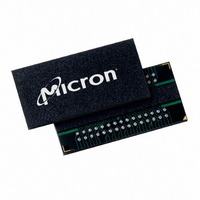
MT46H8M16LFCF-10 IT TR Micron Technology Inc, MT46H8M16LFCF-10 IT TR Datasheet - Page 13

MT46H8M16LFCF-10 IT TR
Manufacturer Part Number
MT46H8M16LFCF-10 IT TR
Description
IC DDR SDRAM 128MBIT 60VFBGA
Manufacturer
Micron Technology Inc
Datasheet
1.MT46H8M16LFCF-10.pdf
(66 pages)
Specifications of MT46H8M16LFCF-10 IT TR
Format - Memory
RAM
Memory Type
Mobile DDR SDRAM
Memory Size
128M (8Mx16)
Speed
100MHz
Interface
Parallel
Voltage - Supply
1.7 V ~ 1.9 V
Operating Temperature
-40°C ~ 85°C
Package / Case
60-VFBGA
Lead Free Status / RoHS Status
Lead free / RoHS Compliant
Figure 5:
Stopping the External Clock
PDF: 09005aef8199c1ec/Source: 09005aef81a19319
MT46H8M16LF_1.fm - Rev. K 7/07 EN
E13
0
0
1
1
E11
E12
0
–
0
1
0
1
Extended Mode Register
E10
Mode Register Definintion
Base Mode Register
Reserved
Extended Mode Register
Reserved
0
–
Notes:
E9
0
–
E8
0
–
1. Change the clock frequency.
2. Stop the clock.
1. On-chip temperature sensor is used in place of TCSR. Setting these bits will have no effect.
One method of controlling the power efficiency in applications is to throttle the clock
which controls the SDRAM. There are two basic ways to control the clock:
Both of these are specific to the application and its requirements and both allow power
savings due to possible less transitions on the clock path.
The Mobile DDR SDRAM allows the clock to change frequency during operation, only if
all the timing parameters are met with respect to that change and all refresh require-
ments are satisfied.
The clock can also be stopped if there are no data accesses in progress, either WRITEs or
READs that would be affected by this change. If a WRITE or a READ is in progress the
entire data burst must be complete prior to stopping the clock.
For READs, a burst completion is defined when the read postamble is satisfied; for
WRITEs, a burst completion is defined when the write postamble and
satisfied. CKE must be held HIGH with CK = LOW and CK# = HIGH for the full duration
of the clock stop mode. One clock cycle and at least one NOP is required after the clock is
restarted before a valid command can be issued. Figure 6 on page 14 illustrates the clock
stop mode.
BA1
E13
13
1
E7
0
–
12
BA0
E12
0
E6–E0
Valid
–
11
A11
E11
set to “0”
10
A10
E10
Operating Mode
Normal Operation
All other states reserved
A9
E9
9
E6
0
0
1
1
A8
E8
8
E5
0
1
0
1
A7
E7
7
A6
E6
6
DS
13
5
A5
E5
TCSR
128Mb: 8 Meg x 16 Mobile DDR SDRAM
4
A4
E4
E2
0
0
0
0
1
1
1
1
Micron Technology, Inc., reserves the right to change products or specifications without notice.
1
A3
E3
3
E1
0
0
1
1
0
0
1
1
A2
2
E2
E0
0
1
0
1
0
1
0
1
PASR
A1
1
E1
Partial Array Self Refresh Coverage
Full Array (All Banks)
Half Array (BA1 = 0)
Quarter Array (BA1 = BA0 = 0)
Reserved
Reserved
Reserved
Reserved
Reserved
A0
0
E0
Address Bus
Extended Mode
Register
©2004 Micron Technology, Inc. All rights reserved.
Register Definition
t
WR or
t
WTR are


