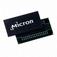
MT46H8M16LFCF-10 IT TR Micron Technology Inc, MT46H8M16LFCF-10 IT TR Datasheet - Page 9

MT46H8M16LFCF-10 IT TR
Manufacturer Part Number
MT46H8M16LFCF-10 IT TR
Description
IC DDR SDRAM 128MBIT 60VFBGA
Manufacturer
Micron Technology Inc
Datasheet
1.MT46H8M16LFCF-10.pdf
(66 pages)
Specifications of MT46H8M16LFCF-10 IT TR
Format - Memory
RAM
Memory Type
Mobile DDR SDRAM
Memory Size
128M (8Mx16)
Speed
100MHz
Interface
Parallel
Voltage - Supply
1.7 V ~ 1.9 V
Operating Temperature
-40°C ~ 85°C
Package / Case
60-VFBGA
Lead Free Status / RoHS Status
Lead free / RoHS Compliant
Register Definition
Mode Registers
Standard Mode Register
Burst Length
PDF: 09005aef8199c1ec/Source: 09005aef81a19319
MT46H8M16LF_1.fm - Rev. K 7/07 EN
Note:
10. Issue NOP or DESELECT commands for at least
7. Using the LOAD MODE REGISTER command, load the standard mode register as
8. Issue NOP or DESELECT commands for at least
9. Using the LOAD MODE REGISTER command, load the extended mode register to the
The Mobile DDR SDRAM has been properly initialized and is ready to receive any valid
command.
The mode registers are used to define the specific mode of operation of the Mobile DDR
SDRAM. There are two mode registers used to specify the operational characteristics of
the device. The standard mode register, which exists for all SDRAM devices, and the
extended mode register, which is exists on all Mobile SDRAM devices.
The standard mode register definition includes the selection of a burst length, a burst
type, a CAS latency and an operating mode, as shown in Figure 3 on page 10. The stan-
dard mode register is programmed via the LOAD MODE REGISTER command (with BA0
= 0 and BA1 = 0) and will retain the stored information until it is programmed again.
Reprogramming the standard mode register will not alter the contents of the memory,
provided it is performed correctly. The mode register must be loaded when all banks are
idle and no bursts are in progress, and the controller must wait the specified time before
initiating the subsequent operation. Violating either of these requirements will result in
unspecified operation.
Mode register bits A0–A2 specify the burst length, A3 specifies the type of burst (sequen-
tial or interleaved), A4–A6 specify the CAS latency, and A7–A11 specify the operating
mode.
Read and write accesses to the Mobile DDR SDRAM are burst oriented, with the burst
length being programmable, as shown in Figure 3 on page 10. The burst length deter-
mines the maximum number of column locations that can be accessed for a given READ
or WRITE command. Burst lengths of 2, 4, or 8 are available for both the sequential and
the interleaved burst types.
Reserved states should not be used, as unknown operation or incompatibility with
future versions may result.
When a READ or WRITE command is issued, a block of columns equal to the burst
length is effectively selected. All accesses for that burst take place within this block,
meaning that the burst will wrap until a boundary is reached. The block is uniquely
selected by A1–Ai when BL = 2, by A2–Ai when BL = 4, by A3–Ai when BL = 8 (where Ai is
desired.
desired operating modes. Note that the sequence in which the standard and extended
mode registers are programmed is not critical.
Standard refers to meeting JEDEC-standard mode register definitions.
9
128Mb: 8 Meg x 16 Mobile DDR SDRAM
Micron Technology, Inc., reserves the right to change products or specifications without notice.
t
t
MRD time.
MRD time.
©2004 Micron Technology, Inc. All rights reserved.
Register Definition


