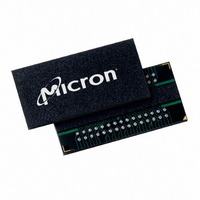
MT46H8M16LFCF-10 IT TR Micron Technology Inc, MT46H8M16LFCF-10 IT TR Datasheet - Page 53

MT46H8M16LFCF-10 IT TR
Manufacturer Part Number
MT46H8M16LFCF-10 IT TR
Description
IC DDR SDRAM 128MBIT 60VFBGA
Manufacturer
Micron Technology Inc
Datasheet
1.MT46H8M16LFCF-10.pdf
(66 pages)
Specifications of MT46H8M16LFCF-10 IT TR
Format - Memory
RAM
Memory Type
Mobile DDR SDRAM
Memory Size
128M (8Mx16)
Speed
100MHz
Interface
Parallel
Voltage - Supply
1.7 V ~ 1.9 V
Operating Temperature
-40°C ~ 85°C
Package / Case
60-VFBGA
Lead Free Status / RoHS Status
Lead free / RoHS Compliant
PDF: 09005aef8199c1ec/Source: 09005aef81a19319
MT46H8M16LF_1.fm - Rev. K 7/07 EN
16. The maximum limit for this parameter is not a device limit. The device will operate
17. This is not a device limit. The device will operate with a negative value, but system
18. It is recommended that DQS be valid (HIGH or LOW) on or before the WRITE
19. MIN (
20. The refresh period equals 64ms. This equates to an average refresh rate of 15.625µs.
21. The I/O capacitance per DQS and DQ byte/group will not differ by more than this
22. The valid data window is derived by achieving other specifications:
23. Referenced to each output group: LDQS with DQ0–DQ7; and UDQS with DQ8–DQ15.
24. This limit is a nominal value and does not result in a fail. CKE is HIGH during
25. To maintain a valid level, the transitioning edge of the input must:
26. The input capacitance per ball group will not differ by more than this maximum
27. CK and CK# input slew rate must be ≥ 1V/ns (2V/ns if measured differentially).
28. DQ and DM input slew rates must not deviate from DQS by more than 10 percent. If
29.
30. READs and WRITEs with auto precharge are not allowed to be issued until
31. Any positive glitch must be less than 1/3 of the clock cycle and not more than +200mV
32. V
33.
34. I
35. CKE must be active (HIGH) during the entire time a REFRESH command is executed.
with a greater value for this parameter, but system performance (bus turnaround) will
degrade accordingly.
performance could be degraded due to bus turnaround.
command.
minimum absolute value for the respective parameter.
ments is the largest multiple of
maximum amount for any given device.
t
with the clock duty cycle and a practical data valid window can be derived. The clock
is allowed a maximum duty cycle variation of 45/55. Functionality is uncertain when
operating beyond a 45/55 ratio.
REFRESH command period (
amount for any given device.
the DQ/DM/DQS slew rate is less than 0.5V/ns, timing must be derated: 50ps must be
added to
4V/ns, functionality is uncertain.
t
device CK and CK# inputs, collectively.
can be satisfied prior to the internal PRECHARGE command being issued.
or 2.0V, whichever is less. Any negative glitch must be less than 1/3 of the clock cycle
and not exceed either -150mV or 1.6V, whichever is more positive.
can not be greater than 1/3 of the cycle rate. V
pulse width ≤ 3ns and the pulse width can not be greater than 1/3 of the cycle rate.
t
That is, from the time the AUTO REFRESH command is registered, CKE must be
active at each rising clock edge, until
DQSQ, and
HP (MIN) is the lesser of
HZ (MAX) will prevail over
DD
b. Reach at least the target AC level.
a. Sustain a constant slew rate from the current AC level through to the target AC
c. After the AC target level is reached, continue to maintain at least the target DC
IH
2N specifies DQ, DQS, and DM to be driven to a valid HIGH or LOW logic level.
level, V
overshoot: V
level, V
t
RC or
t
DS and
IL
t
t
IL
(
RFC) for I
QH (
AC
(
DC
), or V
IH
) or V
t
t
HP -
DH for each 100mv/ns reduction in slew rate. If slew rate exceeds
(MAX) = V
IH
DD
IH
t
(
QHS). The data valid window derates directly proportional
AC
(
t
measurements is the smallest multiple of
DC
CL minimum and
53
).
t
DQSCK (MAX) +
).
t
DD
RFC [MIN]) else CKE is LOW (i.e., during standby).
t
Q + 0.5V for a pulse width ≤ 3ns and the pulse width
CK that meets the maximum absolute value for
128Mb: 8 Meg x 16 Mobile DDR SDRAM
Micron Technology, Inc., reserves the right to change products or specifications without notice.
t
RFC later.
t
t
CH minimum actually applied to the
RPST (MAX) condition.
IL
undershoot: V
t
RAS (MAX) for I
©2004 Micron Technology, Inc. All rights reserved.
IL
(MIN) = -0.5V for a
t
CK that meets the
t
HP (
DD
t
CK/2),
t
RAS (MIN)
measure-
Notes
t
RAS.


