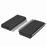
PCF85162T/1,118 NXP Semiconductors, PCF85162T/1,118 Datasheet - Page 18

PCF85162T/1,118
Manufacturer Part Number
PCF85162T/1,118
Description
IC LCD DISPLAY DVR 32SEG 48TSSOP
Manufacturer
NXP Semiconductors
Datasheet
1.PCF85162T1118.pdf
(43 pages)
Specifications of PCF85162T/1,118
Package / Case
48-TSSOP
Display Type
LCD
Configuration
32 Segment
Interface
I²C
Digits Or Characters
Any Digit Type
Current - Supply
8µA
Voltage - Supply
1.8 V ~ 5.5 V
Operating Temperature
-40°C ~ 85°C
Mounting Type
Surface Mount
Number Of Digits
16
Number Of Segments
128
Maximum Clock Frequency
400 KHz
Operating Supply Voltage
1.8 V to 5.5 V
Maximum Power Dissipation
400 mW
Maximum Operating Temperature
+ 85 C
Attached Touch Screen
No
Maximum Supply Current
50 mA
Minimum Operating Temperature
- 40 C
Dc
1123
Lead Free Status / RoHS Status
Lead free / RoHS Compliant
Other names
568-5059-2
NXP Semiconductors
PCF85162_2
Product data sheet
7.13 Output bank selector
7.14 Input bank selector
7.15 Blinker
Once the display RAM of the first PCF85162 has been written, the second PCF85162 is
selected by sending the device-select command again. This time however the command
matches the second device's hardware subaddress. Next the load-data-pointer command
is sent to select the preferred display RAM address of the second PCF85162.
This last step is very important because during writing data to the first PCF85162, the data
pointer of the second PCF85162 is incremented. In addition, the hardware subaddress
should not be changed whilst the device is being accessed on the I
The output bank selector (see
address for transfer to the display register. The actual row selected depends on the
particular LCD drive mode in operation and on the instant in the multiplex sequence.
The PCF85162 includes a RAM bank switching feature in the static and 1:2 multiplex drive
modes. In the static drive mode, the bank-select command may request the contents of
row 2 to be selected for display instead of the contents of row 0. In the 1:2 multiplex mode,
the contents of rows 2 and 3 may be selected instead of rows 0 and 1. This gives the
provision for preparing display information in an alternative bank and to be able to switch
to it once it is assembled.
The input bank selector loads display data into the display RAM in accordance with the
selected LCD drive configuration. Display data can be loaded in row 2 in static drive mode
or in rows 2 and 3 in 1:2 multiplex drive mode by using the bank-select command (see
Table
The display blinking capabilities of the PCF85162 are very versatile. The whole display
can blink at a frequencies selected by the blink-select command (see
frequencies are fractions of the clock frequency. The ratio between the clock and blink
frequencies depends on the blink mode selected (see
An additional feature is for an arbitrary selection of LCD elements to blink. This applies to
the static and 1:2 multiplex drive modes and can be implemented without any
communication overheads. By means of the output bank selector, the displayed RAM
banks are exchanged with alternate RAM banks at the blink frequency. This mode can
also be specified by the blink-select command.
In the 1:3 and 1:4 multiplex modes, where no alternative RAM bank is available, groups of
LCD elements can blink by selectively changing the display RAM data at fixed time
intervals.
•
•
•
•
In 1:4 multiplex mode, all RAM addresses of row 0 are selected, these are followed by
the contents of row 1, 2, and then 3
In 1:3 multiplex mode, rows 0, 1, and 2 are selected sequentially
In 1:2 multiplex mode, rows 0 and 1 are selected
In static mode, row 0 is selected
13). The input bank selector functions independently to the output bank selector.
All information provided in this document is subject to legal disclaimers.
Rev. 02 — 7 May 2010
Table
13) selects one of the four rows per display RAM
Universal LCD driver for low multiplex rates
Table
6).
2
PCF85162
C-bus interface.
Table
© NXP B.V. 2010. All rights reserved.
14). The blink
18 of 43


