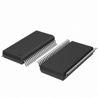
PCF85162T/1,118 NXP Semiconductors, PCF85162T/1,118 Datasheet - Page 26

PCF85162T/1,118
Manufacturer Part Number
PCF85162T/1,118
Description
IC LCD DISPLAY DVR 32SEG 48TSSOP
Manufacturer
NXP Semiconductors
Datasheet
1.PCF85162T1118.pdf
(43 pages)
Specifications of PCF85162T/1,118
Package / Case
48-TSSOP
Display Type
LCD
Configuration
32 Segment
Interface
I²C
Digits Or Characters
Any Digit Type
Current - Supply
8µA
Voltage - Supply
1.8 V ~ 5.5 V
Operating Temperature
-40°C ~ 85°C
Mounting Type
Surface Mount
Number Of Digits
16
Number Of Segments
128
Maximum Clock Frequency
400 KHz
Operating Supply Voltage
1.8 V to 5.5 V
Maximum Power Dissipation
400 mW
Maximum Operating Temperature
+ 85 C
Attached Touch Screen
No
Maximum Supply Current
50 mA
Minimum Operating Temperature
- 40 C
Dc
1123
Lead Free Status / RoHS Status
Lead free / RoHS Compliant
Other names
568-5059-2
NXP Semiconductors
9. Limiting values
PCF85162_2
Product data sheet
CAUTION
Table 15.
In accordance with the Absolute Maximum Rating System (IEC 60134).
[1]
[2]
[3]
[4]
[5]
Symbol Parameter
V
V
V
V
I
I
I
I
I
P
P
V
I
T
T
I
O
DD
DD(LCD)
SS
lu
stg
oper
DD
LCD
I
O
tot
o
ESD
Pass level; Human Body Model (HBM), according to
Pass level; Charged-Device Model (CDM), according to
Pass level; Machine Model (MM), according to
Pass level; latch-up testing according to
According to the NXP store and transport requirements (see
stored at a temperature of +8 °C to +45 °C and a humidity of 25 % to 75 %. For long term storage products
deviant conditions are described in that document.
Static voltages across the liquid crystal display can build up when the LCD supply voltage
(V
display artifacts. To avoid such artifacts, V
LCD
supply voltage
LCD supply voltage
input voltage
output voltage
input current
output current
supply current
LCD supply current
ground supply current
total power dissipation
output power
electrostatic discharge
voltage
latch-up current
storage temperature
operating temperature
) is on while the IC supply voltage (V
Limiting values
All information provided in this document is subject to legal disclaimers.
Rev. 02 — 7 May 2010
Conditions
on each of the pins CLK,
SDA, SCL, SYNC, SA0,
OSC, A0 to A2
on each of the pins S0 to
S31, BP0 to BP3
HBM
CDM
MM
Ref. 8 “JESD78”
Ref. 6 “JESD22-A115”
Universal LCD driver for low multiplex rates
LCD
DD
) is off, or vice versa. This may cause unwanted
and V
Ref. 5
Ref. 7
at maximum ambient temperature (T
DD
“JESD22-A114”.
Ref. 10
must be applied or removed together.
“JESD22-C101”.
“NX3-00092”) the devices have to be
[5]
[1]
[2]
[3]
[4]
Min
−0.5
−0.5
−0.5
−0.5
−10
−10
−50
−50
−50
-
-
-
-
-
-
−65
−40
PCF85162
© NXP B.V. 2010. All rights reserved.
Max
+6.5
+7.5
+6.5
+7.5
+10
+10
+50
+50
+50
400
100
±2000
±1000
±200
200
+150
+85
amb(max)
26 of 43
Unit
V
V
V
V
mA
mA
mA
mA
mA
mW
mW
V
V
V
mA
°C
°C
).


