DK-DEV-4SE530N Altera, DK-DEV-4SE530N Datasheet - Page 43
DK-DEV-4SE530N
Manufacturer Part Number
DK-DEV-4SE530N
Description
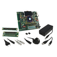
KIT DEV STRATIX IV FPGA 4SE530
Manufacturer
Altera
Series
Stratix® IVr
Type
FPGAr
Datasheet
1.DK-DEV-4SE530N.pdf
(54 pages)
Specifications of DK-DEV-4SE530N
Contents
Board, Cables, CD, DVD, Power Supply
Silicon Manufacturer
Altera
Core Architecture
FPGA
Core Sub-architecture
Stratix
Silicon Core Number
EP4S
Silicon Family Name
Stratix IV E
Rohs Compliant
Yes
For Use With/related Products
EP4SE530
Lead Free Status / RoHS Status
Lead free / RoHS Compliant
Other names
544-2605
Available stocks
Company
Part Number
Manufacturer
Quantity
Price


Chapter 6: Board Test System
Using the Board Test System
© May 2010 Altera Corporation
■
■
■
■
Data Type
The Data type control specifies the type of data contained in the transactions. The
following data types are available for analysis:
■
■
■
Error Control
The Error Ccontrol controls display data errors detected during analysis and allow
you to insert errors:
■
■
■
■
Start
The Start control initiates HSMC transaction performance analysis.
Stop
The Stop control terminates transaction performance analysis.
Performance Indicators
These controls display current transaction performance analysis information collected
since you last clicked Start:
■
■
HSMA x17 LVDS SERDES
HSMA x3 single -ended loopback
HSMB x17 LVDS SERDES
HSMB x3 single-ended loopback
PRBS—Selects pseudo-random bit sequences.
Memory—Selects a generic data pattern stored in the on chip memory of the
Stratix IV E device.
Math—Selects data generated from a simple math function within the FPGA
fabric.
Detected errors—Displays the number of data errors detected in the hardware.
Inserted errors—Displays the number of errors inserted into the transaction
stream.
Insert Error—Inserts a one-word error into the transaction stream each time you
click the button. Insert Error is only enabled during transaction performance
analysis.
Clear—Resets the Detected Eerrors and Inserted errors counters to zeros.
TX and RX performance bars—Show the percentage of maximum theoretical data
rate that the requested transactions are able to achieve.
Tx (MBps) and Rx (MBps)—Show the number of bytes of data analyzed per
second. The HSMC x17 SERDES buses on both HSMC A and HSMC B are 17 bits
wide and clocked using the 125 MHz oscillator with a PLL multiplier of 13,
equating to a 1.625 Gbps per pin, or a 27.625 Gbps bandwidth for each x17
SERDES port. The x3 single-ended data bus is 3 bits wide and clocked using a
100 MHz clock single-data-rate for 100 Mbps per pin, or a 300 Mbps bandwidth
for each x3 single-ended data port.
Stratix IV E FPGA Development Kit User Guide
6–17
Related parts for DK-DEV-4SE530N
Image
Part Number
Description
Manufacturer
Datasheet
Request
R

Part Number:
Description:
KIT DEV ARRIA II GX FPGA 2AGX125
Manufacturer:
Altera
Datasheet:

Part Number:
Description:
KIT DEV CYCLONE III LS EP3CLS200
Manufacturer:
Altera
Datasheet:

Part Number:
Description:
KIT DEV FPGA 2AGX260 W/6.375G TX
Manufacturer:
Altera
Datasheet:

Part Number:
Description:
KIT DEV MAX V 5M570Z
Manufacturer:
Altera
Datasheet:

Part Number:
Description:
KIT DEV STRATIX V FPGA 5SGXEA7
Manufacturer:
Altera
Datasheet:

Part Number:
Description:
KIT DEVELOPMENT STRATIX III
Manufacturer:
Altera
Datasheet:

Part Number:
Description:
KIT DEVELOPMENT STRATIX IV
Manufacturer:
Altera
Datasheet:

Part Number:
Description:
KIT DEV ARRIA GX 1AGX60N
Manufacturer:
Altera
Datasheet:
Part Number:
Description:
KIT STARTER CYCLONE IV GX
Manufacturer:
Altera
Datasheet:
Part Number:
Description:
KIT DEVELOPMENT STRATIX IV
Manufacturer:
Altera
Datasheet:

Part Number:
Description:
CPLD, EP610 Family, ECMOS Process, 300 Gates, 16 Macro Cells, 16 Reg., 16 User I/Os, 5V Supply, 35 Speed Grade, 24DIP
Manufacturer:
Altera Corporation
Datasheet:
Part Number:
Description:
CPLD, EP610 Family, ECMOS Process, 300 Gates, 16 Macro Cells, 16 Reg., 16 User I/Os, 5V Supply, 15 Speed Grade, 24DIP
Manufacturer:
Altera Corporation
Datasheet: