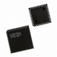
P87C591VFA/00,512 NXP Semiconductors, P87C591VFA/00,512 Datasheet - Page 41

P87C591VFA/00,512
Manufacturer Part Number
P87C591VFA/00,512
Description
IC 80C51 MCU 16K OTP 44-PLCC
Manufacturer
NXP Semiconductors
Series
87Cr
Datasheet
1.P87C591VFA00512.pdf
(160 pages)
Specifications of P87C591VFA/00,512
Core Processor
8051
Core Size
8-Bit
Speed
12MHz
Connectivity
CAN, EBI/EMI, I²C, UART/USART
Peripherals
POR, PWM, WDT
Number Of I /o
32
Program Memory Size
16KB (16K x 8)
Program Memory Type
OTP
Ram Size
512 x 8
Voltage - Supply (vcc/vdd)
4.75 V ~ 5.25 V
Data Converters
A/D 6x10b
Oscillator Type
Internal
Operating Temperature
-40°C ~ 85°C
Package / Case
44-PLCC
Processor Series
P87C5x
Core
80C51
Data Bus Width
8 bit
Data Ram Size
512 B
Interface Type
CAN, I2C, UART
Maximum Clock Frequency
12 MHz
Number Of Programmable I/os
32
Number Of Timers
3
Maximum Operating Temperature
+ 85 C
Mounting Style
SMD/SMT
3rd Party Development Tools
PK51, CA51, A51, ULINK2
Minimum Operating Temperature
- 40 C
On-chip Adc
10 bit, 6 Channel
Lead Free Status / RoHS Status
Lead free / RoHS Compliant
Eeprom Size
-
Lead Free Status / Rohs Status
Details
Other names
568-1256-5
935268182512
P87C591VFAA
935268182512
P87C591VFAA
Available stocks
Company
Part Number
Manufacturer
Quantity
Price
Company:
Part Number:
P87C591VFA/00,512
Manufacturer:
TI
Quantity:
8
Company:
Part Number:
P87C591VFA/00,512
Manufacturer:
NXP Semiconductors
Quantity:
10 000
Philips Semiconductors
12.5.9
The contents of Bus Timing Register 1 defines the length of the bit period, the location of the sample point and the number
of samples to be taken at each bit time. This register can be accessed (read/write) if the Reset Mode is active. In
Operating Mode, this register is read only.
Table 20 Bus Timing Register 1 (BTR1) (CAN address 7)
12.5.9.1
Table 21 Sampling (SAM)
12.5.9.2
TSEG1 and TSEG2 determine the number of clock cycles per bit period and the location of the sample point:
2000 Jul 26
SAM
Single-chip 8-bit microcontroller with CAN controller
handbook, full pagewidth
SAM
BIT
7
CAN:
B
C:
US
Sampling (SAM)
Time Segment 1 (TSEG1) and Time Segment 2 (TSEG2)
T
1 (triple)
0 (once)
IMING
TSEG2.2
t SYNCSEG
sync.
seg.
t scl
6
R
VALUE
EGISTER
t TSEG1
TSEG2.1
1 (BTR1)
t CLK
t TSEG1
TSEG1
t TSEG2
=
nominal bit time
5
t scl
The bus is sampled three times
-> recommended for low/medium speed buses (class A and B) where filtering
The bus is sampled once
-> recommended for high speed buses (SAE class C)
sample point(s)
Fig.12 General structure of a bit period.
=
8 TSEG1.3
spikes on the bus-line is beneficial
t scl
TSEG2.0
baud rate prescaler
t SYNCSEG
4
4 TSEG2.2
+
t TSEG2
TSEG2
4 TSEG1.2
41
TSEG1.3
=
+
1 t scl
2 TSEG2.1
3
sync.
seg.
+
2 TSEG1.1
FUNCTION
+
TSEG1.2
TSEG2.0
e.g.
2
+
TSEG1
TSEG1.0
BRP = 000010b
TSEG1 = 0101b
TSEG2 = 010b
+
1
TSEG1.1
+
1
Preliminary Specification
1
P8xC591
MHI011
TSEG1.0.
0


